2SK1314S
Features
- -
- -
- Low on-resistance High speed switching Low drive current No secondary breakdown Suitable for switching regulator and DC-DC converter
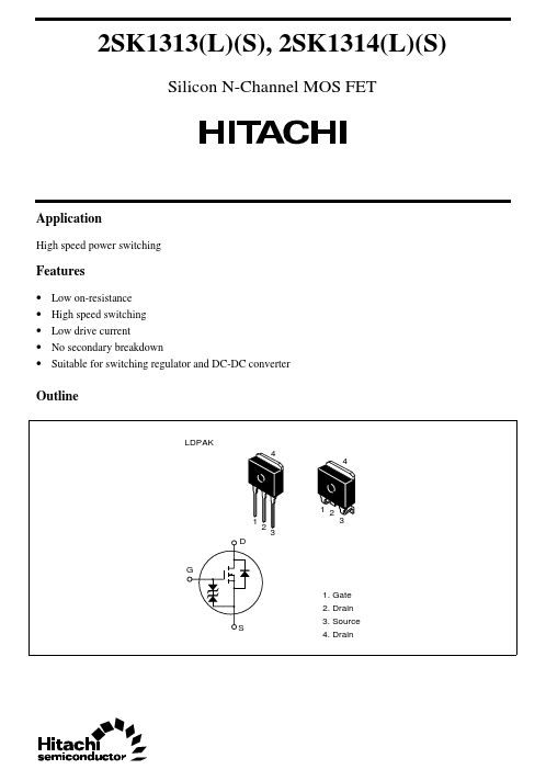
Outline
LDPAK 4 4
1 2 1 D G 2 3
1. Gate 2. Drain 3. Source 4. Drain
2SK1313(L)(S), 2SK1314(L)(S)
Absolute Maximum Ratings (Ta = 25°C)
Item Drain to source voltage 2SK1313 2SK1314 Gate to source voltage Drain current Drain peak current Body to drain diode reverse drain current Channel dissipation Channel temperature Storage temperature Notes: 1. PW ≤ 10 µs, duty cycle ≤ 1% 2. Value at TC = 25°C VGSS ID I D(pulse)- I DR Pch- Tch Tstg
2 1
Symbol VDSS
Ratings 450 500 ±30 5 20 5 50 150
- 55 to +150
Unit V
V A A A W °C °C
2SK1313(L)(S), 2SK1314(L)(S)
Electrical Characteristics (Ta = 25°C)
Item Drain to source breakdown voltage Symbol Min 2SK1313 V(BR)DSS 2SK1314 V(BR)GSS I GSS 450 500 ±30
- -
- -
- - ±10 250 V µA µA I G = ±100 µA, VDS = 0 VGS = ±25 V, VDS = 0 VDS = 360 V, VGS = 0 VDS = 400 V, VGS = 0 VGS(off) 2.0
- - |yfs|...