2SK1315
Key Features
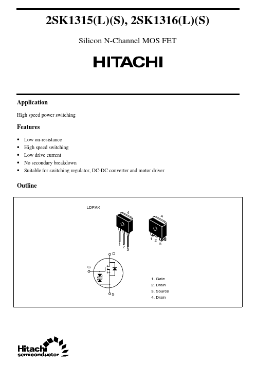
- Low on-resistance High speed switching Low drive current No secondary breakdown Suitable for switching regulator, DC-DC converter and motor driver Outline
| Part Number | Manufacturer | Description |
|---|---|---|
| 2SK1310 | Toshiba | N-Channel MOSFET |
| 2SK1310A | Toshiba | N-Channel MOSFET |
| 2SK1317 | Renesas | Silicon N-Channel MOSFET |
| 2SK1319 | Inchange Semiconductor | N-Channel MOSFET Transistor |