3SK321
Features
- Low noise figure. NF = 2.0 d B typ. at f = 900 MHz
- Capable of low voltage operation
- Provide mini mold packages; MPAK-4R(SOT-143 var.)
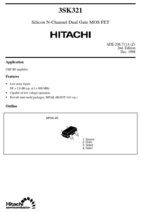
Outline
MPAK-4R
3 4 2 1
1. Source 2. Drain 3. Gate2 4. Gate1
Absolute Maximum Ratings (Ta = 25°C)
Item Drain to source voltage Gate 1 to source voltage Gate 2 to source voltage Drain current Channel power dissipation Channel temperature Storage temperature Symbol VDS VG1S VG2S ID Pch Tch Tstg Ratings 12 ±8 ±8 25 150 150
- 55 to +150 Unit V V V m A m W °C °C
Attention: This device is very sensitive to electro static discharge. It is remended to adopt appropriate cautions when handling this transistor.
Electrical Characteristics (Ta = 25°C)
Item Drain to source breakdown voltage Gate 1 to source breakdown voltage Gate 2 to source breakdown voltage Gate 1 cutoff current Gate 2 cutoff current Drain current Symbol V(BR)DSX V(BR)G1SS V(BR) G2SS I G1SS I G2SS I DS(on) Min 12 ±8 ±8
- - 0.5
- 0.5 0 16 1.2 0.6
- 16
- Typ
- -
- -
- -
- -...