HA22033
HA22033 is GaAs MMIC Low Noise Amplifier for Micro Wave Application manufactured by Hitachi Semiconductor.
Features
- -
- -
- - Suitable for low noise amplifier of Micro Wave Application(1.5 to 1.9GHz) Low voltage and low current operation (2.7V, 1.7m A typ.) Low noise (1.4 d B typ. @1.5GHz) High power gain (14 d B typ. @1.5GHz) Built- in matching circuits (50Ω) Small surface mount package (MPAK- 5)
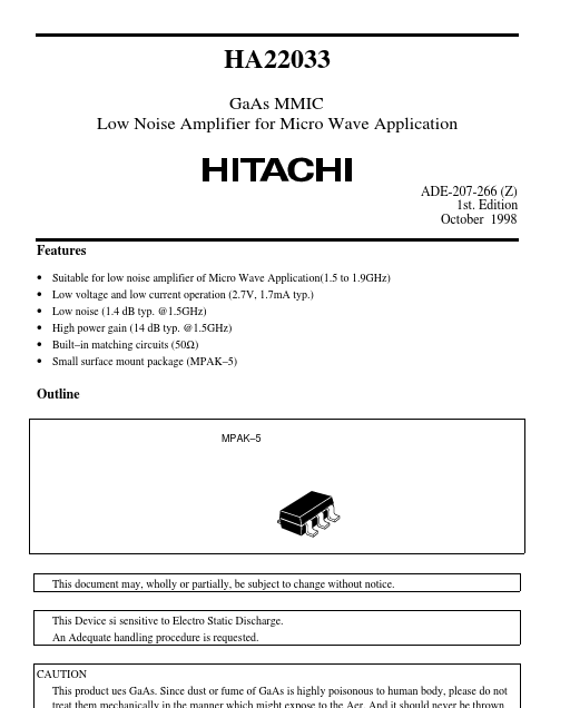
Outline
MPAK- 5
This document may, wholly or partially, be subject to change without notice. This Device si sensitive to Electro Static Discharge. An Adequate handling procedure is requested. CAUTION This product ues Ga As. Since dust or fume of Ga As is highly poisonous to human body, please do not
Absolute Maximum Ratings (Ta = 25°C)
Item Supply voltage Maximum current Power dissipation Channel temperature Storage temperature Operation temperature Maximum input power Symbol Vdd Idd Pd Tch Tstg Topr Pin max Ratings 5 6 100 150
- 55 to +125
- 20 to +70 +15 Unit V m A m W °C °C °C d Bm
Electrical Characteristics (Ta = 25°C, Vdd = 2.7V)
Item Quiescent current Power gain Noise figure Symbol Idd PG NF Min
- 12
- Typ 1.7 14 1.4 Max 2.5
- 2 Unit m A d B d B Test Conditions No signal f = 1.5 GHz f = 1.5 GHz Pin
Typical Performance (Ta = 25°C, Vdd = 2.7V)
Item VSWR (input) VSWR (output) 3rd order intermodulation distortion Symbol VSWR in VSWR out IM3 Typ 1.5 2.2 50 Unit
- - d B Test Conditions f = 1.5 GHz f = 1.5 GHz f = 1.5 GHz, Pin =
- 30 d Bm Pin 4 1
Block Diagram in
1.5p F 4 5.6n H 2 3
Cs 100p F GND
Vdd 5 1 out
100p F
Pin Arrangement
Monthly code (variable) Mark type
Pin name RF out GND Cs RF in Vdd Function RF output Ground RF input Power supply
Top View
Pin No. 1 2 3 4 5
Bypath capacitor (>100 p F)
Pattern Layout scale 4/1 : φ0.5mm : φ0.3mm
Front Side view of PCB Pattern scale 4/1 100p F 5.6n H 1.5p F Vdd GEA RF in cs : Capacitor : Inductor
RF out 100p F
ER=4.8...