HAT2029R
Key Features
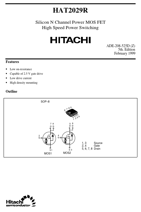
- Low on-resistance Capable of 2.5 V gate drive Low drive current High density mounting
| Part Number | Manufacturer | Description |
|---|---|---|
| HAT2029R | Renesas | Silicon N-Channel Power MOSFET |
| HAT2028R | Renesas | Silicon N-Channel Power MOSFET |
| HAT2028RJ | Renesas | Silicon N-Channel Power MOSFET |
| HAT2022R | Renesas | Silicon N-Channel Power MOSFET |
| HAT2020R | Renesas | Silicon N-Channel Power MOSFET |
| HAT2025R | Renesas | Silicon N-Channel Power MOSFET |
| HAT2027R | Renesas | Silicon N-Channel Power MOSFET |
| HAT2026R | Renesas | Silicon N-Channel Power MOSFET |
| HAT2024R | VBsemi | Dual N-Channel 30-V MOSFET |