HD74AC166
Description
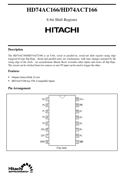
The HD74AC166/HD74ACT166 is an 8-bit, serial or parallel-in, serial-out shift register using edge triggered D-type flip-flops. Serial and parallel entry are synchronous, with state changes initiated by the rising edge of the clock.
Key Features
- Outputs Source/Sink 24 mA