Datasheet4U Logo Datasheet4U.com

HD74ALVCH16827 - 20-bit Buffers / Drivers with 3-state Outputs

General Description

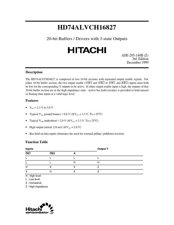
The HD74ALVCH16827 is composed of two 10-bit sections with separated output enable signals.

For either 10-bit buffer section, the two output enable (1OE1 and 1OE2 or 2OE1 and 2OE2) inputs must both be low for the corresponding Y outputs to be active.

Key Features

  • VCC = 2.3 V to 3.6 V.
  • Typical VOL ground bounce < 0.8 V (@VCC = 3.3 V, Ta = 25°C).
  • Typical VOH undershoot > 2.0 V (@VCC = 3.3 V, Ta = 25°C).
  • High output current ±24 mA (@V CC = 3.0 V).
  • Bus hold on data inputs eliminates the need for external pullup / pulldown resistors Function Table Inputs OE1 L L H X H : High level L : Low level X : Immaterial Z : High impedance OE2 L L X H A L H X X L H Z Z Output Y HD74ALVCH16827 Pin Arrangement 1OE1 1 1Y1 2 1.

📥 Download Datasheet

Full PDF Text Transcription (Reference)

The following content is an automatically extracted verbatim text from the original manufacturer datasheet and is provided for reference purposes only.

View original datasheet text
HD74ALVCH16827 20-bit Buffers / Drivers with 3-state Outputs ADE-205-140B (Z) 3rd. Edition December 1999 Description The HD74ALVCH16827 is composed of two 10-bit sections with separated output enable signals. For either 10-bit buffer section, the two output enable (1OE1 and 1OE2 or 2OE1 and 2OE2) inputs must both be low for the corresponding Y outputs to be active. If either output enable input is high, the outputs of that 10-bit buffer section are in the high impedance state. Active bus hold circuitry is provided to hold unused or floating data inputs at a valid logic level. Features • VCC = 2.3 V to 3.6 V • Typical VOL ground bounce < 0.8 V (@VCC = 3.3 V, Ta = 25°C) • Typical VOH undershoot > 2.0 V (@VCC = 3.3 V, Ta = 25°C) • High output current ±24 mA (@V CC = 3.