HD74ALVCH16827
HD74ALVCH16827 is 20-bit Buffers / Drivers manufactured by Renesas.
20-bit Buffers / Drivers with 3-state Outputs
REJ03D0033-0400Z (Previous ADE-205-140B(Z))
Rev.4.00 Oct.02.2003
Description
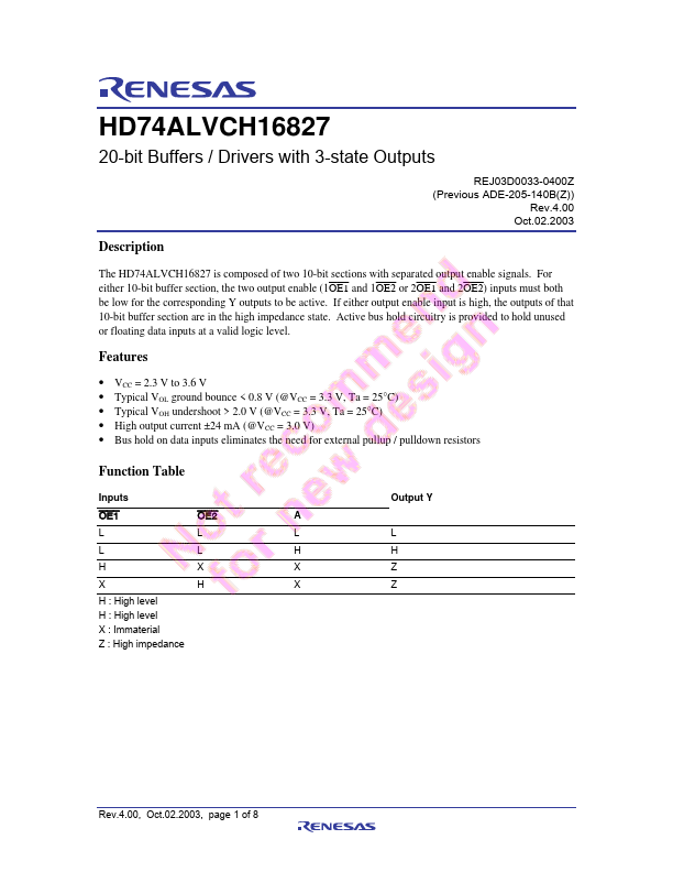
The HD74ALVCH16827 is posed of two 10-bit sections with separated output enable signals. For either 10-bit buffer section, the two output enable (1OE1 and 1OE2 or 2OE1 and 2OE2) inputs must both be low for the corresponding Y outputs to be active. If either output enable input is high, the outputs of that 10-bit buffer section are in the high impedance state. Active bus hold circuitry is provided to hold unused or floating data inputs at a valid logic level.
Features
- VCC = 2.3 V to 3.6 V
- Typical VOL ground bounce < 0.8 V (@VCC = 3.3 V, Ta = 25°C)
-...