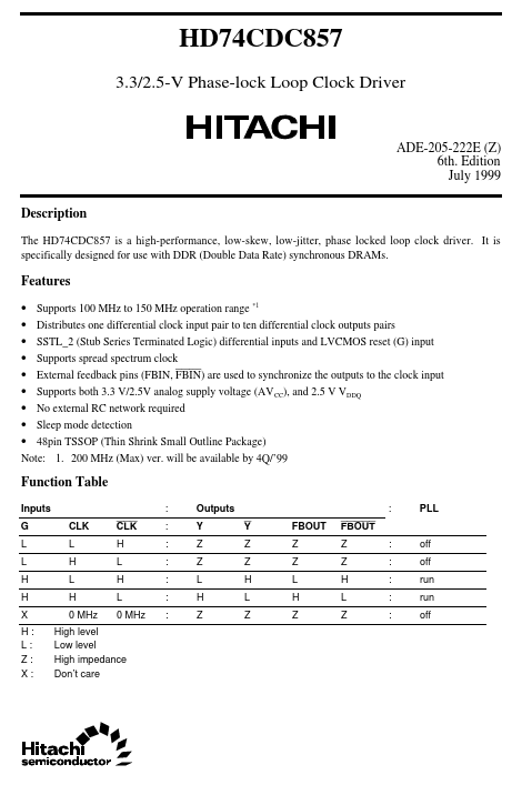
Datasheet4U Logo Datasheet4U.com

HD74CDC857 - 3.3/2.5-V Phase-lock Loop Clock Driver

General Description

The HD74CDC857 is a high-performance, low-skew, low-jitter, phase locked loop clock driver.

It is specifically designed for use with DDR (Double Data Rate) synchronous DRAMs.

Key Features

  • Supports 100 MHz to 150 MHz operation range.
  • 1.
  • Distributes one differential clock input pair to ten differential clock outputs pairs.
  • SSTL_2 (Stub Series Terminated Logic) differential inputs and LVCMOS reset (G) input.
  • Supports spread spectrum clock.
  • External feedback pins (FBIN, FBIN) are used to synchronize the outputs to the clock input.
  • Supports both 3.3 V/2.5V analog supply voltage (AV CC), and 2.5 V VDDQ.
  • No external RC.

📥 Download Datasheet

Full PDF Text Transcription (Reference)

The following content is an automatically extracted verbatim text from the original manufacturer datasheet and is provided for reference purposes only.

View original datasheet text
HD74CDC857 3.3/2.5-V Phase-lock Loop Clock Driver ADE-205-222E (Z) 6th. Edition July 1999 Description The HD74CDC857 is a high-performance, low-skew, low-jitter, phase locked loop clock driver. It is specifically designed for use with DDR (Double Data Rate) synchronous DRAMs. Features • Supports 100 MHz to 150 MHz operation range *1 • Distributes one differential clock input pair to ten differential clock outputs pairs • SSTL_2 (Stub Series Terminated Logic) differential inputs and LVCMOS reset (G) input • Supports spread spectrum clock • External feedback pins (FBIN, FBIN) are used to synchronize the outputs to the clock input • Supports both 3.3 V/2.5V analog supply voltage (AV CC), and 2.