HD74HC259
HD74HC259 is 8-bit Addressable Latch manufactured by Hitachi Semiconductor.
8-bit Addressable Latch
Description
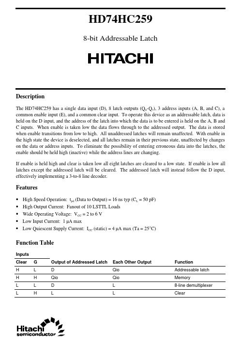
The HD74HC259 has a single data input (D), 8 latch outputs (Q0-Q7), 3 address inputs (A, B, and C), a mon enable input (E), and a mon clear input. To operate this device as an addressable latch, data is held on the D input, and the address of the latch into which the data is to be entered is held on the A, B and C inputs. When enable is taken low the data flows through to the addressed output. The data is stored when enable transitions from low to high. All unaddressed latches will remain unaffected. With enable in the high state the device is deselected, and all latches remain in their previous state, unaffected by changes on the data or address inputs. To eliminate the possibility of entering erroneous data into the latches, the enable should be held high (inactive) while the address lines are changing. If enable is held high and clear is taken low all eight latches are cleared to a low state. If enable is low all latches except the addressed latch will be cleared. The addressed latch will instead follow the D input, effectively implementing a 3-to-8 line decoder.
Features
- -
- -
- High Speed Operation: tpd (Data to Output) = 16 ns typ (CL = 50 p F) High Output Current: Fanout of 10 LSTTL Loads Wide Operating Voltage: VCC = 2 to 6 V Low Input Current: 1 µA max Low Quiescent Supply Current: ICC (static) = 4 µA max (Ta = 25°C)
Function Table
Inputs Clear H H L L G L H L H Output of Addressed Latch D Qio D L Each Other Output Qio Qio L L Function Addressable latch Memory 8-line demultiplexer Clear
Select Inputs C L L L L H H H H B L L H H L L H H A L H L H L H L H Latch Addressed 0 1 2 3 4 5 6 7
Notes: 1. D: the level at the data input 2. Qio: the level of Qi (i = 0, 1,
- -
- 7, as apropriate) before the indicated steady-state input conditions were established.
Pin Arrangement
A Latch select B C Q0 Q1 Outputs Q2 Q3 GND
1 2 3 4 5 6 7 8 B C Q0 Q1 Q2 Q3 Q4 A CLR G D Q7 Q6 Q5
16 VCC 15 Clear 14 Enable...


