The following content is an automatically extracted verbatim text
from the original manufacturer datasheet and is provided for reference purposes only.
View original datasheet text
www.DataSheet4U.com
2SK1169, 2SK1170
Silicon N-Channel MOS FET
Application
High speed power switching
Features
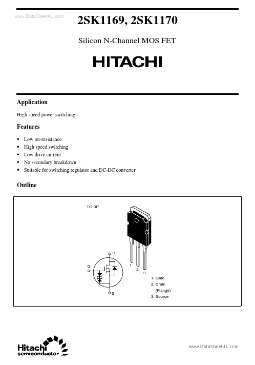
• • • • • Low on-resistance High speed switching Low drive current No secondary breakdown Suitable for switching regulator and DC-DC converter
Outline
TO-3P
D G 1 2 3 1. Gate 2. Drain (Flange) 3. Source
S
2SK1169, 2SK1170 www.DataSheet4U.com
Absolute Maximum Ratings (Ta = 25°C)
Item Drain to source voltage 2SK1169 2SK1170 Gate to source voltage Drain current Drain peak current Body to drain diode reverse drain current Channel dissipation Channel temperature Storage temperature Notes: 1. PW ≤ 10 µs, duty cycle ≤ 1% 2. Value at TC = 25°C VGSS ID I D(pulse)* I DR Pch* Tch Tstg
2 1
Symbol VDSS
Ratings 450 500 ±30 20 80 20 120 150 –55 to +150
Unit V
V A A A W °C °C
2
www.