Datasheet4U.com
🌙
K1626 Datasheet | Hitachi Semiconductor
Part:
K1626
Description:
2SK1626
Manufacturer:
Hitachi Semiconductor
Size:
33.88 KB
K1626 Datasheet (PDF) Download
Related K1626 Datasheets
K1622 Silicon N-Channel MOS FET
K1628 2SK1628
Hitachi Semiconductor
K1626
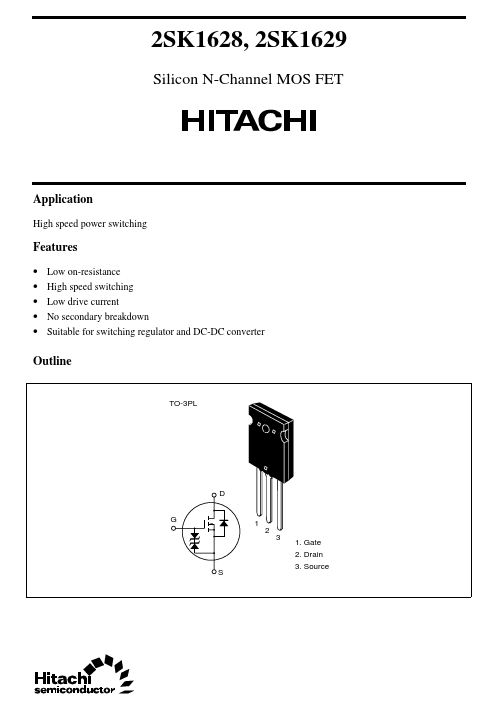
Key Features
Low on-resistance
High speed switching
Low drive current
No secondary breakdown
Suitable for switching regulator and DC-DC converter
×
Close