Hitachi 2SJ181
Silicon P-Channel MOS FET
| Part No. | 2SJ181 |
|---|---|
| Datasheet | 2SJ181 Download |
| Manufacturer |  Hitachi |
| Description | Silicon P-Channel MOS FET |
| Buy | Stock & Price |
FEATURES
●●
●
●
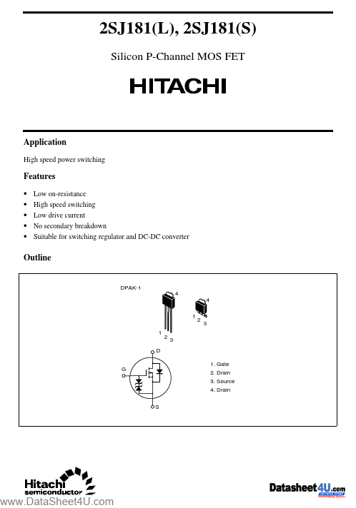
● Low on-resistance High speed switching Low drive current No secondary breakdown Suitable for switching regulator and DC-DC converter Outline DPAK-1 4 4 1 1 D G 1. Gate 2. Drain 3. Source 4. Drain S 2 3 2 3 2SJ181(L), 2SJ181(S)
ABSOLUTE MAXIMUM RATINGS
(Ta = 25°C) Item Drain to source voltage Gate to source voltage Drain current Drain peak current Body to drain diode reverse drain current Channel dissipation Channel temperature Storage temperature Notes: 1. PW ≤ 10 µs, duty cycle ≤ 1% 2. Value at TC = 25°C Symbol VDSS VGSS ID I D(pulse)* I DR Pch* Tch Tstg 2 1 Ratings –600 ±15 –0.5 –1.0 –0.5 20 150 –55 to +150 Unit V V A A A W °C °CELECTRICAL CHARACTERISTICS
(Ta = 25°C) Item Drain to source breakdown voltage Gate to source breakdown voltage Gate to source leak current Symbol Min V(BR)DSS V(BR)GSS I GSS –600 ±15 — — –2.0 — 0.3 — — — — — — — — — Typ — — — — — 15 0.45 220 55 13 7 20 35 35 –0.85 230 Max — — ±10 –100 –4.0 25 — — — — — — — — — — Unit V V µA µA V Ω S pF pF...
