Hitachi 2SJ399
P-Channel MOSFET
| Part No. | 2SJ399 |
|---|---|
| Datasheet | 2SJ399 Download |
| Manufacturer |  Hitachi |
| Description | P-Channel MOSFET |
| Buy | Stock & Price |
FEATURES
●●
●
●
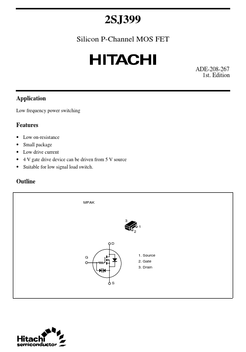
● Low on-resistance Small package Low drive current 4 V gate drive device can be driven from 5 V source Suitable for low signal load switch. Outline MPAK 3 1 2 D 1. Source 2. Gate 3. Drain G S 2SJ399
ABSOLUTE MAXIMUM RATINGS
(Ta = 25°C) Item Drain to source voltage Gate to source voltage Drain current Drain peak current Body to drain diode reverse drain current Channel dissipation Channel temperature Storage temperature Notes: 1. PW ≤ 100 µs, duty cycle ≤ 10% 2. Marking is “ZF–” Symbol VDSS VGSS ID I D(pulse)* I DR Pch Tch Tstg 1 Ratings –30 ±20 –0.2 –0.4 –0.2 150 150 –55 to +150 Unit V V A A A mW °C °CELECTRICAL CHARACTERISTICS
(Ta = 25°C) Item Drain to source breakdown voltage Gate to source breakdown voltage Gate to source leak current Symbol V(BR)DSS V(BR)GSS I GSS Min –30 ±20 — — –1.0 — — Input capacitance Output capacitance Reverse transfer capacitance Turn-on delay time Rise time Turn-off delay time Fall time Ciss Coss Crss t d(on) tr t d(off) tf — — — — — — —...
