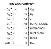
74HC595
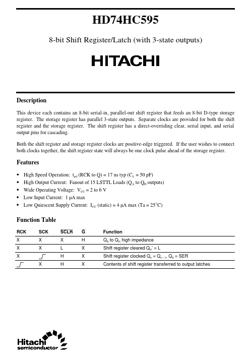
Description
This device each contains an 8-bit serial-in, parallel-out shift register that feeds an 8-bit D-type storage register.
Representative 74HC595 image (package may vary by manufacturer)
This device each contains an 8-bit serial-in, parallel-out shift register that feeds an 8-bit D-type storage register.
Representative 74HC595 image (package may vary by manufacturer)
| Part Number | Manufacturer | Description |
|---|---|---|
| 74HC595 | NXP Semiconductors | 8-bit serial-in serial or parallel-out shift register |
| 74HC595 | Diodes Incorporated | 8-BIT SHIFT REGISTER |
| 74HC595D | Slkor Micro Semicon | high-speed Silicon Gate CMOS device |
| 74HC595 | SG Micro | 8-Bit Serial-In/Serial-Out or Parallel-Out Shift Register |
| 74HC595-Q100 | Nexperia | serial or parallel-out shift register |
| 74HC595A | Motorola Semiconductor | 8-Bit Serial-Input/Serial or Parallel-Output Shift Register |
| 74HC595D | Nexperia | serial or parallel-out shift register |
| 74HC595 | Texas Instruments | 8-Bit Shift Registers |
| 74HC595 | Nexperia | serial or parallel-out shift register |
| 74HC595S16 | Diodes Incorporated | 8-BIT SHIFT REGISTER |