DESCRIPTION
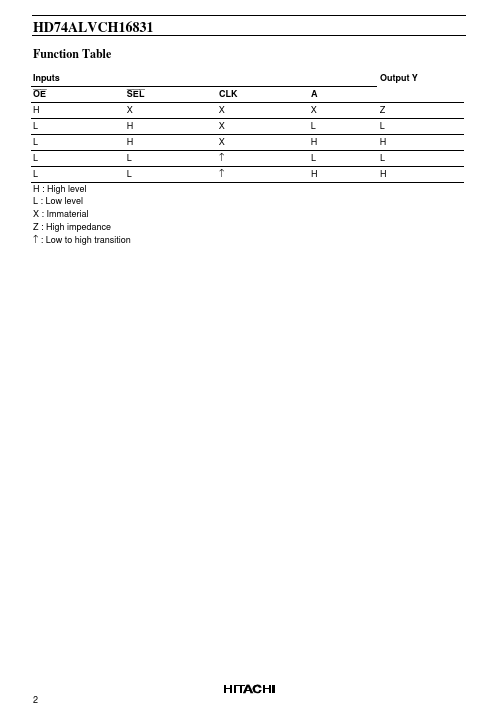
This 1-bit to 4-bit address register / driver is designed for 2.3 V to 3.6 V VCC operation. The device is ideal for use in applications in which a single address bus is driving four separate memory locations. Each OE controls two groups of nine outputs. When SEL is logic low, the device is in the register mode. The register is an edge triggered D-type flip flop. On the positive transition of the clock (CLK) input, data set up at the A inputs is stored in the internal registers. OE controls operate the same as in buffer mode. When OE is logic low, the outputs are in a normal logic state (high or low logic level). When OE is logic high, the outputs are in the high impedance state. To ensure the high impedance state during power up or power down, OE should be tied to V CC through a pullup registor; the minimum value of the registor is determined by the current sinking capability of the driver. SEL and OE do not affect the internal operation of the flip flops. Old data can be retained or new data can be entered while the outputs are in the high impedance state. Hitachi