Hitachi HD74CDCV857
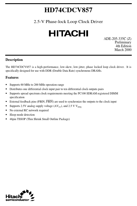
The HD74CDCV857 is a high-performance, low-skew, low-jitter, phase locked loop clock driver. It is specifically designed for use with DDR (Double Data Rate) synchronous DRAMs. CLK provides the clock signal to be distributed by the HD74CDCV857 clock driver.| Part No. | HD74CDCV857 |
|---|---|
| Datasheet | HD74CDCV857 Download |
| Manufacturer |  Hitachi |
| Description | 2.5-V Phase-lock Loop Clock Driver |
| Buy | Stock & Price |
DESCRIPTION
FEATURES
● Supports 60 MHz to 200 MHz operation range● Distributes one differential clock input pair to ten differential clock outputs pairs
● Supports spread spectrum clock requirements meeting the PC100 SDRAM registered DIMM specification
● External feedback pins (FBIN, FBIN) are used to synchronize the outputs to the clock input
● Supports 2.5V analog supply voltage (AVCC), and 2.5 V VDDQ
● No external RC network required
● Sleep mode detection
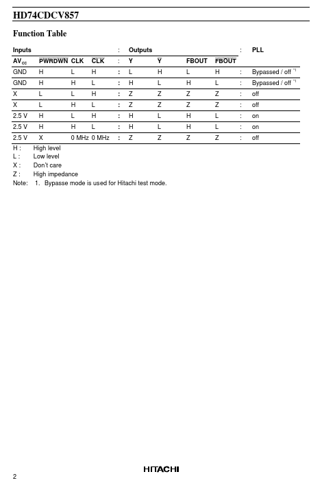
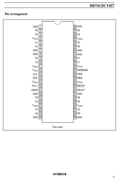
● 48pin TSSOP (Thin Shrink Small Outline Package) HD74CDCV857 Function Table Inputs AV CC GND GND X X 2.5 V 2.5 V 2.5 V H: L: X: Z: Note: PWRDWN CLK H H L L H H X L H L H L H CLK H L H L H L : : : : : : : : : Outputs Y L H Z Z H H Z Y H L Z Z L L Z FBOUT L H Z Z H H Z FBOUT H L Z Z L L Z : : : : : : : Bypassed / off Bypassed / off off off on on off *1 *1 : PLL 0 MHz 0 MHz High level Low level Don’t care High impedance 1. Bypasse mode is used for Hitachi test mode. 2 HD74CDCV857 Pin Arrangement GND 1 Y0 2 Y0 3 V DDQ 4 Y1 5 Y1 6 GN...