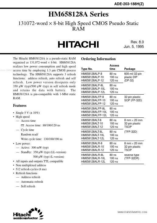
HM658128A
HM658128A is 131072-word x 8-bit High Speed CMOS Pseudo Static RAM manufactured by Hitachi Semiconductor.
Features
- Single 5 V (± 10%)
- High speed
- Access time CE Access time: 80/100/120 ns
- Cycle time Random read/ Write cycle time: 130/160/190 ns
- Low power:
- Active: 300 m W (typ)
- Standby: 350 µW (typ) (LL-version) 500 µW (typ) (L-version)
- All inputs and outputs TTL patible
- Non multiplexed address
- 512 refresh cycles (8 ms)
- Refresh functions
- Address refresh
- Automatic refresh
- Self refresh
8 mm × 20 mm 32-pin plastic TSOP reverse type (TFP-32DR)
HM658128A Series
Pin Arrangement
HM658128ALP/ALFP Series
RFSH A16 A14 A12 A7 A6 A5 A4 A3 1 2 3 4 5 6 7 8 9 10 11 12 13 14 15 16 32 31 30 29 28 27 26 25 24 23 22 21 20 19 18 17 VCC A15 CS WE A13 A8 A9 A11 OE A10 CE I/O 7 I/O 6 I/O 5 I/O 4 I/O 3
..
A2 A1 A0 I/O 0 I/O 1 I/O 2 VSS
(Top View)
HM658128ALT Series
A11 A9 A8 A13 WE CS A15 VCC RFSH A16 A14 A12 A7 A6 A5 A4 1 2 3 4 5 6 7 8 9 10 11 12 13 14 15 16 32 31 30 29 28 27 26 25 24 23 22 21 20 19 18 17 OE A10 CE I/O 7 I/O 6 I/O 5 I/O 4 I/O 3 VSS I/O 2 I/O 1 I/O 0 A0 A1 A2 A3
(Top View)
HM658128A Series
Pin Arrangement (cont)
HM658128ALR Series A4 A5 A6 A7 A12 A14 A16 RFSH VCC A15 CS WE A13 A8 A9 A11 16 15 14 13 12 11 10 9 8 7 6 5 4 3 2 1 (Top View) 17 18 19 20 21 22 23 24 25 26 27 28 29 30 31 32 A3 A2 A1 A0 I/O0 I/O1 I/O2 VSS I/O3 I/O4 I/O5 I/O6 I/O7 CE A10 OE
..
Pin Description
Symbol A0 to A16 I/O0 to I/O7 RFSH CE OE WE CS VCC VSS Pin name Address inputs Data input/output Refresh Chip enable Output enable Write enable Chip select Power supply Ground
HM658128A Series
Block Diagram
A0
Address latch control
Row decoder
Memory matrix (512 × 256) ×...