2SD1470
2SD1470 is Silicon NPN Epitaxial Planar Transistor manufactured by Hitachi Semiconductor.
Silicon NPN Epitaxial, Darlington
Application
Low frequency power amplifier
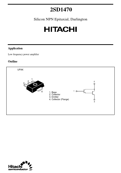
Outline
UPAK
1 3 2
1. Base 2. Collector 3. Emitter 4. Collector (Flange)
Absolute Maximum Ratings (Ta = 25°C)
Item Collector to base voltage Collector to emitter voltage Emitter to base voltage Collector current Collector peak current Collector power dissipation Junction temperature Storage temperature Symbol VCBO VCEO VEBO IC i C(peak)- PC
- Tj Tstg
2 1
Ratings 60 60 7 1 2 1 150
- 55 to +150
Unit V V V A A W °C °C
Notes: 1. PW ≤ 10 ms, Duty cycle ≤ 20% 2. Value on the alumina ceramic board (12.5 x 30 x 0.7 mm)
Electrical Characteristics (Ta = 25°C)
Item Collector to base breakdown voltage Symbol V(BR)CBO Min 60 60 7
- - 2000
- - Typ
- -
- -
- -
- - Max
- -
- 10 10 100000 1.5 2.0 V V Unit V V V µA µA Test conditions I C = 10 µA, IE = 0 I C = 1 m A, RBE = ∞ I E = 10 µA, IC = 0 VCB = 60 V, IE = 0 VEB = 7 V, IC = 0 VCE = 3 V, IC = 0.5 A- 1 I C = 500 m A, IB = 0.5 m A- 1 I C = 500 m A, IB = 0.5 m A- 1
Collector to emitter breakdown V(BR)CEO voltage Emitter to base breakdown voltage Collector cutoff current Emitter cutoff current DC current transfer ratio Collector to emitter saturation voltage Base to emitter saturation voltage Notes: 1. Pulse test 2. Marking is “AT”. V(BR)EBO I CBO I EBO h FE VCE(sat) VBE(sat)
Maximum Collector Dissipation Curve 1.2 Collector Power Dissipation PC (W) (on the alumina ceramic board) Collector Current IC (A) 10 3 1.0 0.3 0.1 0.03 0.01 0 50 100 150 Ambient Temperature Ta (°C) 3 10 30 100 1,000 Collector to Emitter Voltage VCE (V) i C(peak) Area of Safe Operation
1 µs
µs 0 s s 10 m m 1 10 =
Ta = 25°C 1Shot Pulse
Typical Output Characteristics Ta = 25°C
DC Current Transfer Ratio vs. Collector Current DC Current Transfer Ratio h FE (×103) 300
Collector Current IC (A)
20 18 16 14 12 10...