2SD1676
2SD1676 is NPN Silicon Transistor manufactured by Hitachi Semiconductor.
..
Silicon NPN with Internal Resistance
Application
Low frequency amplifier, Muting, Switching, Inverter
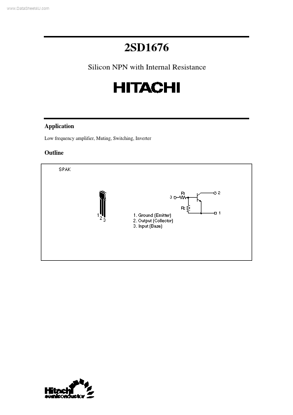
Outline
Absolute Maximum Ratings (Ta = 25°C)
Item Supply voltage Input voltage Output current Total power dissipation Operating temperature Storage temperature Symbol VCC VI IO PT TOP Tstg Ratings 20 ±10 600 300
- 25 to +110
- 55 to +150 Unit V V m A m W °C °C
Electrical Characteristics (Ta = 25°C)
Item Input on voltage Input off voltage Output saturation voltage Output cutoff current DC current transfer ratio Input resistance Resistance ratio Turn on time Storage time Fall time Output on resistance Symbol VI(on) VI(off) VO(on) I O(off) Gi R1 R1/R2 t on t stg tf ron Min 1.1 0.5
- - 60
- 0.9
- -
- - Typ
- - 20
- 100 6.8 1.0 0.3 1.5 0.7 1.0 Max 1.7 1.2 40 0.5
- - 1.1
- -
- - µS µS µS Ω VI = 7 V, RL = 1kΩ, f = 1k Hz VCC = 5 V, VI = 5 V, RL = 1kΩ kΩ Unit V V m V µA Test conditions VCC = 0.2 V, IO = 10 m A VCC = 5 V, IO = 10 µA I O = 10 m A, II = 0.5 m A VCC = 5 V, VI = 0 VCC = 5 V, IO = 10 m A
When using this document, keep the following in mind: 1. This document may, wholly or partially, be subject to change without notice. 2. All rights are reserved: No one is permitted to reproduce or duplicate, in any form, the whole or part of this document without Hitachi’s permission. 3. Hitachi will not be held responsible for any damage to the user that may result from accidents or any other reasons during operation of the user’s unit according to this document. 4. Circuitry and other examples described herein are meant merely to indicate the characteristics and performance of Hitachi’s semiconductor products. Hitachi assumes no responsibility for any intellectual property claims or other problems that may result from applications based on the examples described herein. 5. No license is granted by implication or otherwise under any patents or other rights of any third party or Hitachi, Ltd. 6. MEDICAL APPLICATIONS: Hitachi’s...