2SK2569
2SK2569 is Silicon N-Channel MOSFET manufactured by Hitachi Semiconductor.
Features
- -
- - Low on-resistance. R DS(on) = 2.6 max. (at V GS = 4 V, I D = 100m A) 2.5V gate drive device. Small package (MPAK).
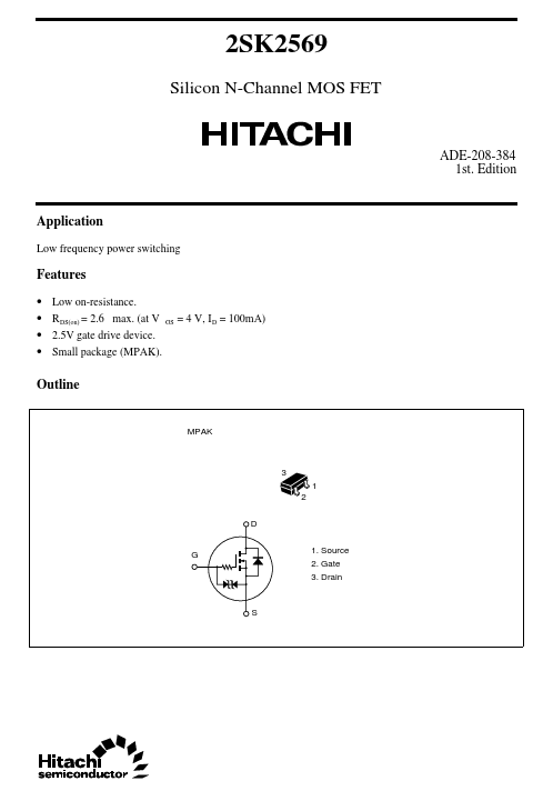
Outline
MPAK
3 1 2 D 1. Source 2. Gate 3. Drain
Absolute Maximum Ratings (Ta = 25°C)
Item Drain to source voltage Gate to source voltage Drain current Drain peak current Channel dissipation Channel temperature Storage temperature Notes 1. PW ≤ 10 µs, duty cycle ≤ 1 % Symbol VDSS VGSS ID I D(pulse)- Pch- Tch Tstg
2 1
Ratings 50 ±20 0.2 0.4 150 150
- 55 to +150
Unit V V A A m W °C °C
Electrical Characteristics (Ta = 25°C)
Item Drain to source breakdown voltage Gate to source breakdown voltage Symbol V(BR)DSS V(BR)GSS Min 50 ±20
- - 0.5
- - 0.13
- -
- -
- -
- Typ
- -
- -
- 2.0 3.1 0.23 14.0 17.2 1.73 40 86 1120 430 Max
- - 1.0 ±2.0 1.5 2.6 5.0
- -
- -
- -
- - Unit V V µA µA V Ω Ω S p F p F p F µs µs µs µs Test Conditions I D = 100 µA, VGS = 0 I G = ±100 µA, VDS = 0 VDS = 40 V, VGS = 0 VGS = ±16 V, VDS = 0 I D = 10 µA, VDS = 5 V I D = 100 m A VGS = 4 V- 1 I D = 40 m A VGS = 2.5 V- 1 I D = 100 m A VDS = 10 V VDS = 10 V VGS = 0 f = 1 MHz VGS = 10 V, ID = 100 m A RL = 300 Ω
Zero gate voltage drain current I DSS Gate to source leak current Gate to source cutoff voltage Static drain to source on state resistance Static drain to source on state resistance Foward transfer admittance Input capacitance Output capacitance Reverse transfer capacitance Turn-on delay time Rise time Turn-off delay time Fall time Notes 1. Pulse Test 2. Marking is "ZN- " I GSS VGS(off) RDS(on)1 RDS(on)2 |yfs| Ciss Coss Crss t d(on) tr t d(off) tf
Maximum Channel Dissipation Curve 200 Pch (m W) Maximum Safe Operation Area 1 ms 0.3 150 I D (A) 0.1
PW = 10 s m
Channel Dissipation
Drain Current
0.03 0.01
Operation in this area is limited by R DS(on) pe ra tio n
0.003 0.001 Ta = 25 °C 0.1 0.3...