BB504C
BB504C is Build in Biasing Circuit MOS FET IC VHF&UHF RF Amplifier manufactured by Hitachi Semiconductor.
Features
..
- Build in Biasing
- -
- -
Circuit; To reduce using parts cost & PC board space. Low noise; NF = 1.0 d B typ. at f = 200 MHz,NF =1.75 d B typ. at f =900 MHz High gain; PG = 30 d B typ. at f = 200 MHz, PG = 22 d B typ. at f = 900 MHz Withstanding to ESD; Build in ESD absorbing diode. Withstand up to 200 V at C = 200 p F, Rs = 0 conditions. Provide mini mold packages; CMPAK-4 (SOT-343mod)
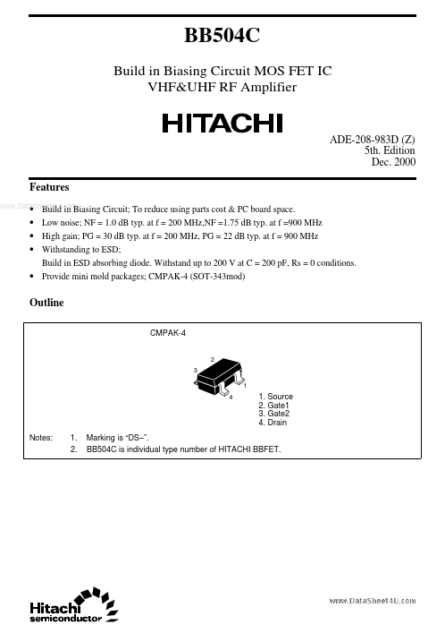
Outline
CMPAK-4
2 3 1 4
1. Source 2. Gate1 3. Gate2 4. Drain
Notes:
1. 2.
Marking is “DS- ”. BB504C is individual type number of HITACHI BBFET.
Absolute Maximum Ratings (Ta = 25°C)
Item Drain to source voltage Gate1 to source voltage Gate2 to source voltage Drain current Channel power dissipation Channel temperature Storage temperature
..
Symbol VDS VG1S VG2S ID Pch Tch Tstg
Ratings 6 +6
- 0 +6
- 0 30 100 150
- 55 to +150
Unit V V V m A m W °C °C
Electrical Characteristics (Ta = 25°C)
Item Drain to source breakdown voltage Gate1 to source breakdown voltage Gate2 to source breakdown voltage Symbol V(BR)DSS V(BR)G1SS V(BR)G2SS Min 6 +6 +6
- - 0.6 0.6 13 24 1.7 1.0
- 25
- 17
- Typ
- -
- -
- 0.85 0.85 16 29 2.1 1.4 0.027 30 1.0 22 1.75 Max
- -
- +100 +100 1.1 1.1 19 34 2.5 1.8 0.05
- 1.8
- 2.3 Unit V V V n A n A V V m A m S p F p F p F d B d B d B d B Test Conditions I D = 200µA, VG1S = VG2S = 0 I G1 = +10 µA, VG2S = VDS = 0 I G2 = +10 µA, VG1S = VDS = 0 VG1S = +5V, V G2S = VDS = 0 VG2S = +5V, V G1S = VDS = 0 VDS = 5V, VG2S = 4V, ID = 100µA VDS = 5V, VG1S = 5V, ID = 100µA VDS = 5V, VG1 = 5V VG2S = 4V, RG = 120kΩ VDS = 5V, VG1 = 5V, VG2S =4V RG = 120kΩ, f = 1k Hz VDS = 5V, VG1 = 5V VG2S =4V, RG = 120kΩ f = 1MHz VDS = 5V, VG1 = 5V VG2S =4V, RG = 120kΩ f = 200MHz VDS = 5V, VG1 = 5V VG2S =4V, RG = 120kΩ f = 900MHz
Gate1 to source cutoff current I G1SS Gate2 to source cutoff current I G2SS Gate1 to source cutoff voltage VG1S(off) Gate2 to source cutoff voltage VG2S(off) Drain current Forward transfer admittance Input capacitance Output capacitance Reverse transfer capacitance Power...