HD74ACT107
HD74ACT107 is Dual JK Flip-Flop (with Separate Clear and Clock) manufactured by Hitachi Semiconductor.
Description
The HD74AC107/HD74ACT107 dual JK master/slave flip-flops have a separate clock for each flip-flop. Inputs to the master section are controlled by the clock pulse. The clock pulse also regulates the state of the coupling transistors which connect the master and slave sections. The sequence of operation is as follows: 1) isolate slave from master; 2) enter information from J and K inputs to master; 3) disable J and K inputs; 4) transfer information from master to slave.
Features
- Outputs Source/Sink 24 m A
- HD74ACT107 has TTL-patible Inputs
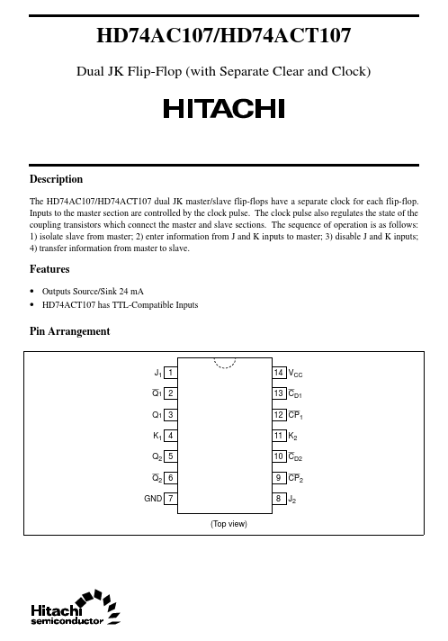
Pin Arrangement
J1 1 Q1 2 Q1 3 K1 4 Q2 5 Q2 6 GND 7 (Top view)
14 VCC 13 CD1 12 CP1 11 K2 10 CD2 9 CP2 8 J2
HD74AC107/HD74ACT107
Logic Symbol
3 8 9 Q1 2 11
1 12 4
J1 CP1 K1
Q1
J2 CP2 K2
Q2
CD1 13
CD2 10
Q2
VCC = Pin14 GND = Pin7
Pin Names
J1, J2, K1, K2 CP1, CP2 C D1, CD2 Q1, Q2, Q1, Q 2 Data Inputs Clock Pulse Inputs (Active Falling Edge) Direct Clear Inputs (Active Low) Outputs
Truth Table
Inputs @ tn J L L H H H L tn tn + 1 : : : : K L H L H High Voltage Level Low Voltage Level Bit time before clock pulse. Bit time after clock pulse. Outputs @ tn + 1 Q Qn L H Qn
HD74AC107/HD74ACT107
Logic Diagram
CD J K CP #CP CP #CP Q #CP #CP Q
CP CP CP CP
DC Characteristics (unless otherwise specified)
Item Maximum quiescent supply current Maximum quiescent supply current Maximum additional ICC/input (HD74ACT107) Symbol I CC I CC I CCT Max 80 8.0 1.5 Unit µA µA m A Condition VIN = VCC or ground, VCC = 5.5 V, Ta = Worst case VIN = VCC or ground, VCC = 5.5 V, Ta = 25°C VIN = VCC
- 2.1 V, VCC = 5.5 V Ta = Worst case
HD74AC107/HD74ACT107
AC Characteristics: HD74AC107
Ta = +25°C CL = 50 p F Item Maximum clock frequency Propagation delay CP to Q or Q Propagation delay CP to Q or Q Propagation delay CD to Q Propagation delay CD to Q Note: t PHL t PLH t PHL t PLH Symbol f max VCC (V)- 1 3.3 5.0 3.3 5.0 3.3 5.0 3.3 5.0 3.3 5.0 1. Voltage Range 3.3 is 3.3 V ± 0.3 V Voltage Range 5.0 is 5.0 V ± 0.5 V Min 125...