HD74CDC857
HD74CDC857 is 3.3/2.5-V Phase-lock Loop Clock Driver manufactured by Hitachi Semiconductor.
Description
The HD74CDC857 is a high-performance, low-skew, low-jitter, phase locked loop clock driver. It is specifically designed for use with DDR (Double Data Rate) synchronous DRAMs.
Features
- Supports 100 MHz to 150 MHz operation range
- 1
- Distributes one differential clock input pair to ten differential clock outputs pairs
- SSTL_2 (Stub Series Terminated Logic) differential inputs and LVCMOS reset (G) input
- Supports spread spectrum clock
- External feedback pins (FBIN, FBIN) are used to synchronize the outputs to the clock input
- Supports both 3.3 V/2.5V analog supply voltage (AV CC), and 2.5 V VDDQ
- No external RC network required
- Sleep mode detection
- 48pin TSSOP (Thin Shrink Small Outline Package) Note: 1. 200 MHz (Max) ver. will be available by 4Q/’99
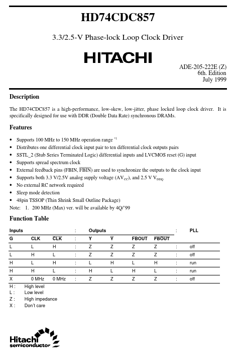
Function Table
Inputs G L L H H X H: L: Z: X: CLK L H L H 0 MHz CLK H L H L 0 MHz : : : : : : : Outputs Y Z Z L H Z Y Z Z H L Z FBOUT Z Z L H Z FBOUT Z Z H L Z : : : : : off off run run off : PLL
High level Low level High impedance Don’t care
Pin Arrangement
GND 1 Y0 2 Y0 3 V DDQ 4 Y1 5 Y1 6 GND 7 GND 8 Y2 9 Y2 10 V DDQ 11 V DDQ 12 CLK 13 CLK 14 V DDQ 15 AV CC 16 AGND 17 GND 18 Y3 19 Y3 20 V DDQ 21 Y4 22 Y4 23 GND 24
48 GND 47 Y5 46 Y5 45 V DDQ 44 Y6 43 Y6 42 GND 41 GND 40 Y7 39 Y7 38 V DDQ 37 G 36 FBIN 35 FBIN 34 V DDQ 33 FBOUT 32 FBOUT 31 GND 30 Y8 29 Y8 28 V DDQ 27 Y9 26 Y9 25 GND
(Top view)
Absolute Maximum Ratings
Item Supply voltage Input voltage Output voltage
- 1
Symbol VDDQ VI VO I IK I OK IO
Ratings
- 0.5 to 4.6
- 0.5 to 4.6
- 0.5 to VDDQ +0.5
- 50
- 50 ±50 ±100 0.7
Unit V V V m A m A m A m A W °C
Conditions
Input clamp current Output clamp current Continuous output current
VI < 0 VO < 0 VO = 0 to VDDQ
Supply current through each V DDQ or GND I VDDQ or IGND Maximum power dissipation at Ta = 55°C (in still air) Storage temperature Notes: Tstg
- 65 to +150
Stresses beyond those listed under “absolute maximum ratings” may cause permanent damage to the device....