HD74HCT449
HD74HCT449 is Quad. Bus Transceivers with Individual Direction Controls manufactured by Hitachi Semiconductor.
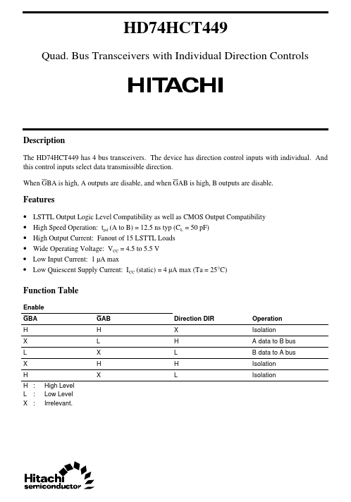
Description
The HD74HCT449 has 4 bus transceivers. The device has direction control inputs with individual. And this control inputs select data transmissible direction. When GBA is high, A outputs are disable, and when GAB is high, B outputs are disable.
Features
- -
- -
- - LSTTL Output Logic Level patibility as well as CMOS Output patibility High Speed Operation: tpd (A to B) = 12.5 ns typ (CL = 50 p F) High Output Current: Fanout of 15 LSTTL Loads Wide Operating Voltage: VCC = 4.5 to 5.5 V Low Input Current: 1 µA max Low Quiescent Supply Current: ICC (static) = 4 µA max (Ta = 25°C)
Function Table
Enable GBA H X L X H H : L : X : High Level Low Level Irrelevant. GAB H L X H X Direction DIR X H L H L Operation Isolation A data to B bus B data to A bus Isolation Isolation
Pin Arrangement
GBA 1 A1 2 DIR2 3 A2 4 A3 5 DIR3 6 A4 7 GND 8 (Top view)
16 VCC 15 GAB 14 B1 13 DIR1 12 B2 11 B3 10 DIR4 9 B4
Logic Diagram
DIR1
A1
B1
To other three transceivers
Absolute Maximum Ratings
Item Supply voltage range Input voltage Output voltage DC current drain per pin DC current drain per VCC, GND DC input diode current DC output diode current Power dissipation per package Storage temperature Symbol VCC VIN VOUT I OUT I CC, I GND I IK I OK PT Tstg Rating
- 0.5 to +7.0
- 0.5 to VCC + 0.5
- 0.5 to VCC + 0.5 ±35 ±75 ±20 ±20 500
- 65 to +150 Unit V V V m A m A m A m A m W °C
DC Characteristics
Ta = 25°C Item Input voltage Symbol VIH VIL Output voltage VOH Ta =
- 40 to +85°C Max
- 0.8
- - 0.1 0.33 ±5.0 ±1.0 40 µA µA µA V Unit V V V Test Conditions VCC (V) 4.5 to 5.5 4.5 to 5.5 4.5 4.5 4.5 4.5 5.5 5.5 5.5 Vin = VIH or VIL I OH =
- 20 µA I OH =
- 6 m A Vin = VIH or VIL I OL = 20 µA I OL = 6 m A Vin = VIH or VIL, Vout = VCC or GND Vin = VCC or GND Vin = VCC or GND, Iout = 0 µA
Min Typ Max Min 2.0
- 4.4
- -
- - 2.0
- -
- 4.4 4.13
-...