HY27UA081G1M
HY27UA081G1M is (HY27SAxxx) 1Gbit (128Mx8bit / 64Mx16bit) NAND Flash Memory manufactured by SK Hynix.
- Part of the HY27SAxxx comparator family.
- Part of the HY27SAxxx comparator family.
description of Device Operations
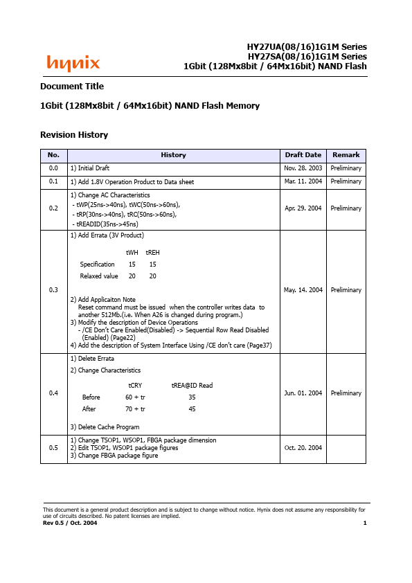
- /CE Don’t Care Enabled(Disabled) -> Sequential Row Read Disabled (Enabled) (Page22) 4) Add the description of System Interface Using /CE don’t care (Page37) 1) Delete Errata 2) Change Characteristics 0.4 t CRY Before After 60 + tr 70 + tr t REA@ID Read 35 45 Jun. 01. 2004 Preliminary 15 20 t REH 15 20 May. 14. 2004 Preliminary Apr. 29. 2004 Preliminary
History
Draft Date
Nov. 28. 2003 Mar. 11. 2004
Remark
Preliminary Preliminary
3) Delete Cache Program 0.5 1) Change TSOP1, WSOP1, FBGA package dimension 2) Edit TSOP1, WSOP1 package figures 3) Change FBGA package figure Oct. 20. 2004
This document is a general product description and is subject to change without notice. Hynix does not assume any responsibility for use of circuits described. No patent licenses are implied. Rev 0.5 / Oct. 2004 1
HY27UA(08/16)1G1M Series HY27SA(08/16)1G1M Series 1Gbit (128Mx8bit / 64Mx16bit) NAND Flash FEATURES
SUMMARY
HIGH DENSITY NAND FLASH MEMORIES
- Cost effective solutions for mass storage applications
FAST BLOCK ERASE
- Block erase time: 2ms (Typ)
NAND INTERFACE
- x8 or x16 bus width.
- Multiplexed Address/ Data
- Pinout patibility for all densities
STATUS REGISTER ELECTRONIC SIGNATURE
SUPPLY VOLTAGE
Sequential Row Read Option
: HY27UAXX1G1M
- 3.3V device: VCC = 2.7 to 3.6V
1.8V Operation Product : TBD
AUTOMATIC PAGE 0 READ AT POWER-UP OPTION
- Boot from NAND support
- Automatic Memory Download
- 1.8V device: VCC = 1.7 to 1.95V : HY27SAXX1G1M
Memory Cell Array
- 1056Mbit = 528 Bytes x 32 Pages x 8,192 Blocks
SERIAL NUMBER OPTION HARDWARE DATA PROTECTION
- Program/Erase locked during Power transitions
PAGE SIZE
- x8 device: (512 + 16 spare) Bytes : HY27(U/S)A081G1M
- x16 device: (256 + 8 spare) Words : HY27(U/S)A161G1M
DATA INTEGRITY
- 100,000 Program/Erase cycles
- 10 years Data Retention
BLOCK...