Datasheet Summary
HY5DU28422A(L)T HY5DU28822A(L)T HY5DU281622A(L)T
3rd 128M DDR SDRAM
HY5DU28422A(L)T HY5DU28822A(L)T HY5DU281622A(L)T
This document is a general product description and is subject to change without notice. Hynix semiconductor does not assume any responsibility for use of circuits described. No patent licenses are implied. Rev. 0.4/May. 02 1
..
HY5DU28422A(L)T HY5DU28822A(L)T HY5DU281622A(L)T
Revision History
1. Revision 0.2 (Nov.01) 1) Device operation and timing diagram removed 2) tHZ / tLZ SPEC defined 2. Revision 0.3 (Feb.02) 1) “Preliminary” removed 3. Revision 0.4 (May. 02) 1) Input leakage current changed from +/-5uA to +/-2uA
Rev. 0.4/May. 02
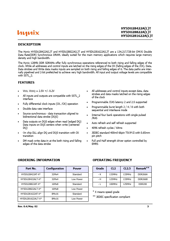
HY5DU28422A(L)T...