HY62256A
HY62256A is 32K x 8-Bit CMOS SRAM manufactured by Hyundai.
DESCRIPTION
The HY62256A is a high-speed, low power and 32,786 x 8-bits CMOS Static Random Access Memory fabricated using Hyundai's high performance CMOS process technology. The HY62256A has a data retention mode that guarantees data to remain valid at the minimum power supply voltage of 2.0 volt. Using the CMOS technology, supply voltages from 2.0 to 5.5volt has little effect on supply current in the data retention mode. The HY62256A is suitable for use in low voltage operation and battery back-up application. Product Voltage Speed No. (V) (ns) HY62256A 5.0 55/70/85 Note 1. Current value is max. Operation Current(m A) 50
FEATURES
Fully static operation and Tri-state output TTL patible inputs and outputs Low power consumption Battery backup(L/LL-part)
- 2.0V(min.) data retention
- Standard pin configuration
- 28 pin 600 mil PDIP
- 28 pin 330mil SOP
- 28 pin 8x13.4 mm TSOP-I (Standard and Reversed)
- -
- -
Standby Current(u A) L LL 1m A 100 25
Temperature (°C) 0~70(Normal)
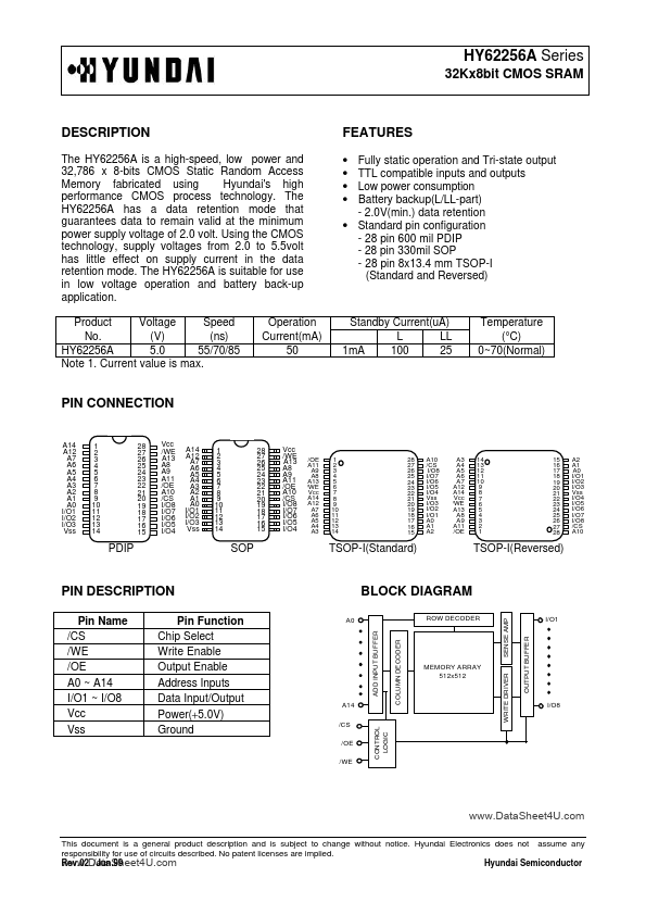
PIN CONNECTION
A14 A12 A7 A6 A5 A4 A3 A2 A1 A0 I/O1 I/O2 I/O3 Vss Vcc /WE A13 A8 A9 A11 /OE A10 /CS I/O8 I/O7 I/O6 I/O5 I/O4
1 2 3 4 5 6 7 8 9 10 11 12 13 14
28 27 26 25 24 23 22 21 20 19 18 17 16 15
A14 A12 A7 A6 A5 A4 A3 A2 A1 A0 I/O1 I/O2 I/O3 Vss
1 2 3 4 5 6 7 8 9 10 11 12 13 14
28 27 26 25 24 23 22 21 20 19 18 17 16 15
Vcc /WE A13 A8 A9 A11 /OE A10 /CS I/O8 I/O7 I/O6 I/O5 I/O4
/OE A11 A9 A8 A13 /WE Vcc A14 A12 A7 A6 A5 A4 A3
1 2 3 4 5 6 7 8 9 10 11 12 13 14
28 27 26 25 24 23 22 21 20 19 18 17 16 15
A10 /CS I/O8 I/O7 I/O6 I/O5 I/O4 Vss I/O3 I/O2 I/O1 A0 A1 A2
A3 A4 A5 A6 A7 A12 A14 Vcc /WE A13 A8 A9 A11 /OE
14 13 12 11 10 9 8 7 6 5 4 3 2 1
15 16 17 18 19 20 21 22 23 24 25 26 27 28
A2 A1 A0 I/O1 I/O2 I/O3 Vss I/O4 I/O5 I/O6 I/O7 I/O8 /CS A10
PDIP
TSOP-I(Standard)
TSOP-I(Reversed)
PIN DESCRIPTION
Pin Name /CS /WE /OE A0 ~ A14 I/O1 ~ I/O8 Vcc Vss Pin Function Chip Select Write Enable Output Enable Address Inputs Data Input/Output Power(+5.0V) Ground
A0
BLOCK DIAGRAM
SENSE...