ICS557-01 Overview
Description
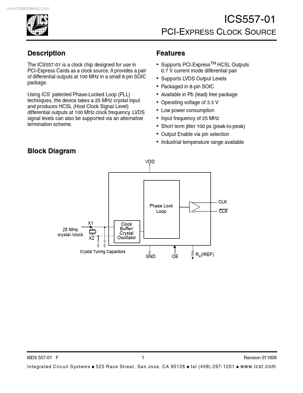
The ICS557-01 is a clock chip designed for use in PCI-Express Cards as a clock source. It provides a pair of differential outputs at 100 MHz in a small 8-pin SOIC package.
Key Features
- Supports PCI-ExpressTM HCSL Outputs 0.7 V current mode differential pair