ICS557-01 Overview
Description
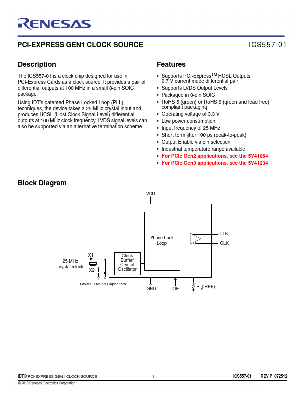
The ICS557-01 is a clock chip designed for use in PCI-Express Cards as a clock source. It provides a pair of differential outputs at 100 MHz in a small 8-pin SOIC package.
Key Features
- Supports PCI-ExpressTM HCSL Outputs 0.7 V current mode differential pair
- Supports LVDS Output Levels
- Packaged in 8-pin SOIC
- RoHS 5 (green) or RoHS 6 (green and lead free) compliant packaging
- Operating voltage of 3.3 V
- Low power consumption
- Input frequency of 25 MHz
- Short term jitter 100 ps (peak-to-peak)
- Output Enable via pin selection
- Industrial temperature range available