ICS85357-01
ICS85357-01 is LVPECL / ECL CLOCK MULTIPLEXER manufactured by ICST.
..
Integrated Circuit Systems, Inc.
4:1 OR 2:1 DIFFERENTIAL-TO-3.3V LVPECL / ECL CLOCK MULTIPLEXER
Features
- High speed differential multiplexer. The device can be configured as either a 4:1 or 2:1 multiplexer
- 1 differential 3.3V LVPECL output
- 4 selectable CLK, n CLK inputs
- CLK, n CLK pair can accept the following differential input levels: LVDS, LVPECL, LVHSTL, SSTL, HCSL
- Maximum output frequency up to 750MHz
- Translates any single ended input signal to 3.3V LVPECL levels with resistor bias on n CLKx input
- Part-to-part skew: 150ps (maximum)
- Propagation delay: 1.5ns (maximum)
- LVPECL mode operating voltage supply range: VCC = 3.135V to 3.465V, VEE = 0V
- ECL mode operating voltage supply range: VCC = 0V, VEE = -3.135V to -3.465V
- 0°C to 70°C ambient operating temperature
- Industrial temperature information available upon request
GENERAL DESCRIPTION
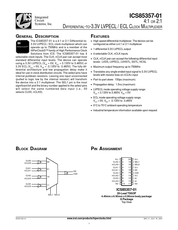
The ICS85357-01 is a 4:1 or 2:1 Differential-to3.3V LVPECL / ECL clock multiplexer which can Hi Per Clock S™ operate up to 750MHz and is a member of the Hi Per Clock S™ family of High Performance Clock Solutions from ICS. The ICS85357-01 has 4 selectable clock inputs. The CLK, n CLK pair can accept most standard differential input levels. The device can operate using a 3.3V LVPECL (VEE = 0V, VCC = 3.135V to 3.465V) or 3.3V ECL (VCC = 0V, VEE = -3.135V to -3.465V). The fully differential architecture and low propagation delay make it ideal for use in clock distribution circuits. The select pins have internal pulldown resistors. Leaving one input unconnected (pulled to logic low by the internal resistor) will transform the device into a 2:1 multiplexer. The SEL1 pin is the most significant bit and the binary number applied to the select pins will select the same numbered data input (i.e., 00 selects CLK0, n CLK0).
,&6
BLOCK DIAGRAM
CLK0 n CLK0 CLK1 n CLK1 CLK2 n CLK2 CLK3 n CLK3 00
PIN ASSIGNMENT
VCC CLK0 n CLK0 CLK1 n CLK1 CLK2 n CLK2 CLK3 n CLK3 VEE 1 2 3 4 5 6 7 8 9 10 20 19 18 17 16 15...