MK2308-2
MK2308-2 is ZERO DELAY LOW SKEW BUFFER manufactured by ICST.
Description
The MK2308-2 is a low jitter, low skew, high performance Phase-Lock Loop (PLL) based zero delay buffer for high speed applications. Based on ICS’ proprietary low jitter PLL techniques, the device provides eight low skew outputs at speeds up to 160 MHz at 3.3 V. The MK2308-2 includes a bank of four outputs running at 1/2X. In the zero delay mode, the rising edge of the input clock is aligned with the rising edges of all eight outputs. pared to petitive CMOS devices, the MK2308-2 has the lowest jitter.
Features
- -
- -
- -
- Packaged in 16-pin SOIC Zero input-output delay Four 1X outputs plus four 1/2X outputs Output to output skew is less than 250 ps Output clocks up to 160 MHz at 3.3 V Ability to generate 2X the input Full CMOS outputs with 18 m A output drive capability at TTL levels at 3.3 V spectrum clock generators
- Spread Smart TM technology works with spread
- Advanced, low power, sub micron CMOS process
- Operating voltage of 3.3 V or 5 V
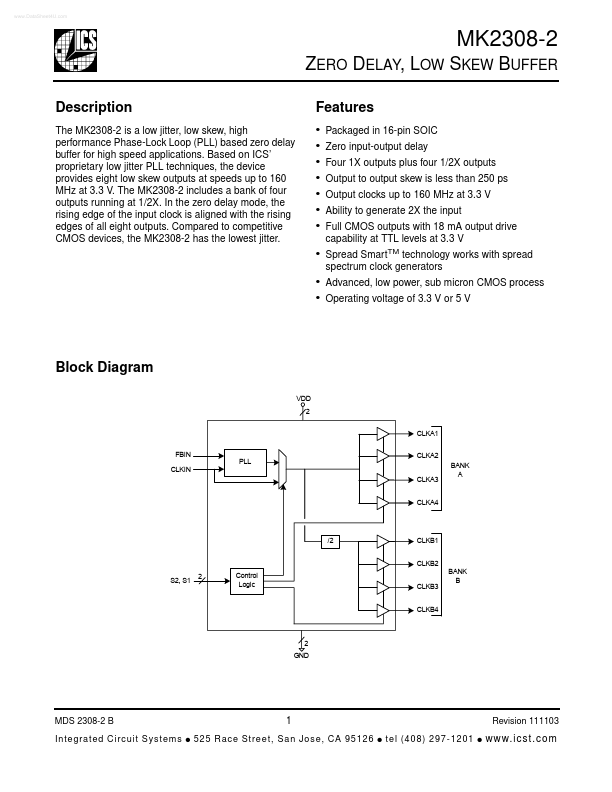
Block Diagram
VDD 2 CLKA1 FBIN CLKIN CLKA2 CLKA3 CLKA4 BANK A
/2
CLKB1 CLKB2
S2, S1
Control Logic
CLKB3 CLKB4
BANK B
2 GND
MDS 2308-2 B I n t e gra te d C i r c u i t S y s t e m s
- 1
525 Race Stre et, San Jo se, CA 9 5126
- Revision 111103 te l (40 8) 2 97-12 01
- w w w. i c st . c o m
MK2308-2 ZERO DELAY, LOW SKEW BUFFER
Pin Assignment
CLKIN CLKA1 CLKA2 VDD GND CLKB1 CLKB2 S2 1 2 3 4 5 6 7 8 16 15 14 13 12 11 10 9 FBIN CLKA4 CLKA3 VDD GND CLKB4 CLKB3 S1
Feedback Configuration Table
Feedback From Bank A Bank B CLKA1:A4 CLKIN 2XCLKIN CLKB1:B4 CLKIN/2 CLKIN
16-pin (150 mil) SOIC
Output Clock Mode Select Table
S2 0 0 1 1 S1 0 1 0 1 Clocks A1:A4 Tri-state (high impedance) Running Running Running Clocks B1:B4 Tri-state (high impedance) Tri-state (high impedance) Running Running Internet Generation None PLL Buffer only (no zero delay) PLL PLL Status On On Off On
Pin Descriptions
Pin Number 1 2-3 4 5 6-7 8 9 10
- 11 12 13 14
- 15 16 Pin Name CLKIN CLKA1:A4 VDD GND CLKB1:B4 S2 S1 CLKB1:B4...