9DB833 Overview
Description
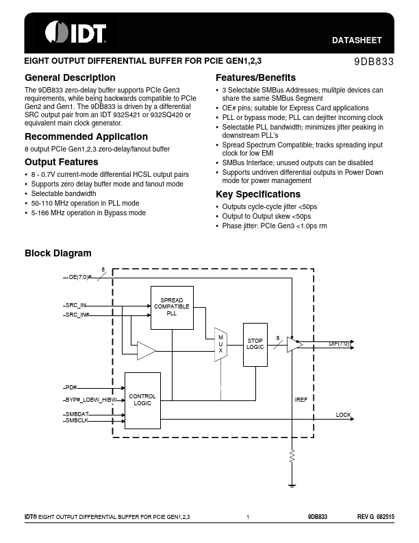
The 9DB833 zero-delay buffer supports PCIe Gen3 requirements, while being backwards compatible to PCIe Gen2 and Gen1. The 9DB833 is driven by a differential SRC output pair from an IDT 932S421 or 932SQ420 or equivalent main clock generator.
Key Features
- 8 - 0.7V current-mode differential HCSL output pairs
- Supports zero delay buffer mode and fanout mode
- Selectable bandwidth
- 50-110 MHz operation in PLL mode
- 5-166 MHz operation in Bypass mode Features/Benefits
- 3 Selectable SMBus Addresses; mulitple devices can share the same SMBus Segment
- OE# pins; suitable for Express Card applications
- PLL or bypass mode; PLL can dejitter incoming clock
- Selectable PLL bandwidth; minimizes jitter peaking in downstream PLL's
- Spread Spectrum Compatible; tracks spreading input clock for low EMI