9DB836
9DB836 is 8-Output 3.3V HCSL PCIe Buffer manufactured by Renesas.
Description
The 9DB836 is a zero delay/fanout buffer for PCI Express™ clocking. It supports PCIe Gen1- 3 in zero-delay mode and PCIe Gen1- 4 in fanout mode. The 9DB836 is a pin-patible upgrade to the 9DB833 and 9DB834 with a Safe Power Sequence (SPS) clock input.
Typical Applications
- Riser cards
- Storage
- Networking
- JBOD
Output Features
- Eight 0.7V current-mode differential HCSL output pairs
- Supports zero delay buffer (ZDB) mode and fanout mode
- Selectable bandwidth for zero delay mode
- 50- 110 MHz operation in PLL mode
- 5- 166 MHz operation in Bypass mode
Features
- SPS internal receiver bias network keeps input clock parked when input is floating
- Supports both 85Ω and 100Ω output impedance with appropriate resistor selection
- OE# pins default to controlling outputs
- PLL or Bypass mode; PLL can dejitter ining clock
- Selectable PLL bandwidth; minimizes jitter peaking in downstream PLLs
- Spread spectrum patible
- Outputs default to Hi-Z when disabled or when device is powered down
- SMBus interface; unused outputs can be disabled
- 3 selectable SMBus addresses
Key Specifications
- PCIe Gen3 jitter < 0.6ps rms in ZDB mode
- PCIe Gen4 additive jitter < 0.1ps rms in fanout mode
- Output cycle-to-cycle jitter < 50ps
- Output-to-output skew < 50ps
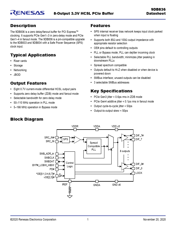
Block Diagram
VDDR
VDDA
VDD x5
SRC_IN# SRC_IN
SMB_ADR_tri SMBCLK SMBDAT
BYP#_LOBW_HIBW PD#
^OE[0:1,3:4,6,7]# 8 v OE[2,5]#
Control Logic
IREF
Spread...
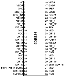
Representative 9DB836 image (package may vary by manufacturer)