Datasheet Summary
12-Output Differential Buffer for PCIe Gen3
9DB1233 Datasheet
Description
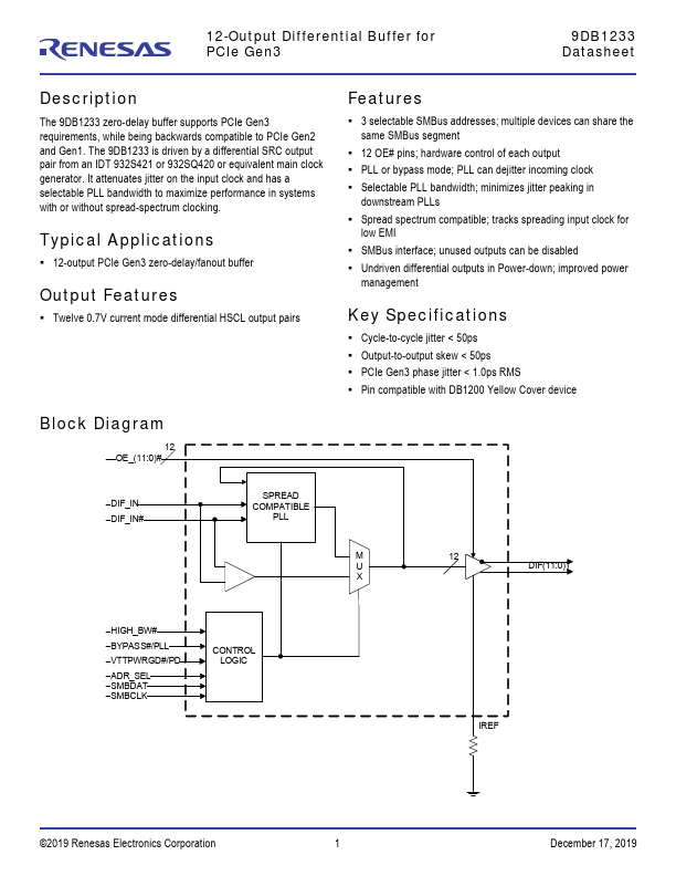
The 9DB1233 zero-delay buffer supports PCIe Gen3 requirements, while being backwards patible to PCIe Gen2 and Gen1. The 9DB1233 is driven by a differential SRC output pair from an IDT 932S421 or 932SQ420 or equivalent main clock generator. It attenuates jitter on the input clock and has a selectable PLL bandwidth to maximize performance in systems with or without spread-spectrum clocking.
Typical Applications
- 12-output PCIe Gen3 zero-delay/fanout buffer
Output Features
- Twelve 0.7V current mode differential HSCL output pairs
Features
- 3 selectable SMBus addresses; multiple devices can share the same SMBus...