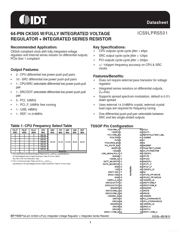
Datasheet4U Logo Datasheet4U.com

9LPRS501 - ICS9LPRS501

Product Overview

📥 Download Datasheet

Datasheet preview – 9LPRS501

Datasheet Details

Part number 9LPRS501
Manufacturer IDT
File Size 244.67 KB
Description ICS9LPRS501
Datasheet download datasheet 9LPRS501 Datasheet
Additional preview pages of the 9LPRS501 datasheet.

Product details

Description

PIN # PIN NAME TYPE DESCRIPTION 3.3V PCI clock output or Clock Request control A for either SRC0 or SRC2 pair The power-up default is PCI0 output, but this pin may also be used as a Clock Request control of SRC pair 0 or SRC pair 2 via SMBus.Before configuring this pin as a Clock Request Pin, the PCI output must first be disabled in byte 2, bit 0 of SMBus address space .After the PCI output is disabled (high-Z), the pin can then be set to serve as a Clock Request pin for either SRC pair 2 or p

Features

Other Datasheets by IDT
Published: |