IDT723652
IDT723652 is (IDT7236x2) CMOS SyncBiFIFO manufactured by IDT.
..
CMOS Sync Bi FIFOTM 2,048 x 36 x 2 4,096 x 36 x 2 8,192 x 36 x 2
IDT723652 IDT723662 IDT723672
Features
- -
- -
- -
- -
- -
- Memory storage capacity: IDT723652
- 2,048 x 36 x 2 IDT723662
- 4,096 x 36 x 2 IDT723672
- 8,192 x 36 x 2 Supports clock frequencies up to 83MHz Fast access times of 8ns Free-running CLKA and CLKB may be asynchronous or coincident (simultaneous reading and writing of data on a single clock edge is permitted) Two independent clocked FIFOs buffering data in opposite directions Mailbox bypass register for each FIFO Programmable Almost-Full and Almost-Empty flags Microprocessor Interface Control Logic FFA/IRA, EFA/ORA, AEA, and AFA flags synchronized by CLKA FFB/IRB, EFB/ORB, AEB, and AFB flags synchronized by CLKB
- -
- Select IDT Standard timing (using EFA, EFB, FFA and FFB flags functions) or First Word Fall Through timing (using ORA, ORB, IRA and IRB flag functions) Available in 132-pin Plastic Quad Flatpack (PQFP) or space-saving 120-pin Thin Quad Flatpack (TQFP) Pin patible to the lower density parts, IDT723622/723632/723642 Industrial temperature range (- 40° C to +85°C) is available
DESCRIPTION
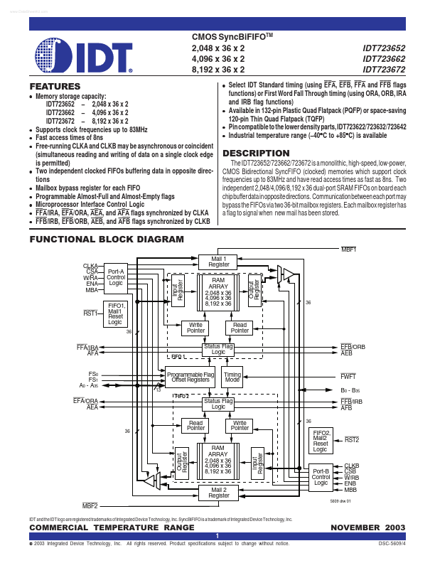
The IDT723652/723662/723672 is a monolithic, high-speed, low-power, CMOS Bidirectional Sync FIFO (clocked) memories which support clock frequencies up to 83MHz and have read access times as fast as 8ns. Two independent 2,048/4,096/8,192 x 36 dual-port SRAM FIFOs on board each chip buffer data in opposite directions. munication between each port may bypass the FIFOs via two 36-bit mailbox registers. Each mailbox register has a flag to signal when new mail has been stored.
FUNCTIONAL BLOCK DIAGRAM
MBF1 CLKA CSA W/RA ENA MBA Mail 1 Register
Input Register Output Register
Port-A Control Logic
RST1
FIFO1, Mail1 Reset Logic
RAM ARRAY 2,048 x 36 4,096 x 36 8,192 x 36
Write Pointer
Read Pointer EFB/ORB AEB
FFA/IRA AFA
FIFO 1
Status Flag Logic
FS0 FS1...