IDT8P34S1212I
Overview
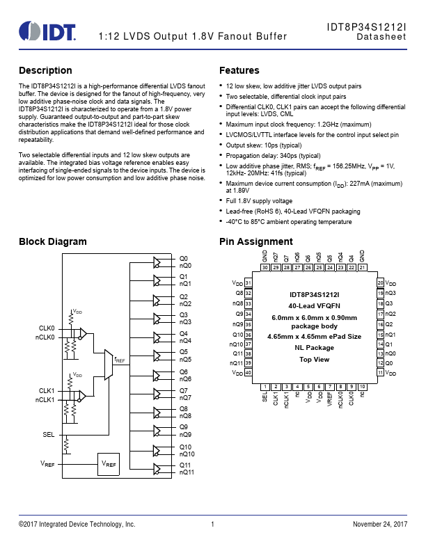
The IDT8P34S1212I is a high-performance differential LVDS fanout buffer. The device is designed for the fanout of high-frequency, very low additive phase-noise clock and data signals.
- 12 low skew, low additive jitter LVDS output pairs
- Two selectable, differential clock input pairs
- Differential CLK0, CLK1 pairs can accept the following differential input levels: LVDS, CML
- Maximum input clock frequency: 1.2GHz (maximum)
- LVCMOS/LVTTL interface levels for the control input select pin
- Output skew: 10ps (typical)
- Propagation delay: 340ps (typical)
- Low additive phase jitter, RMS; fREF = 156.25MHz, VPP = 1V, 12kHz- 20MHz: 41fs (typical)
- Maximum device current consumption (IDD): 227mA (maximum) at 1.89V
- Full 1.8V supply voltage