IN74ACT109
IN74ACT109 is Dual J-K Positive-Edge-Triggered Flip-Flop manufactured by IK Semiconductor.
TECHNICAL DATA
Dual J-K Flip-Flop with Set and Reset
High-Speed Silicon-Gate CMOS
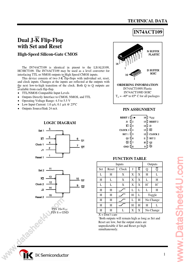
The IN74ACT109 is identical in pinout to the LS/ALS109, HC/HCT109. The IN74ACT109 may be used as a level converter for interfacing TTL or NMOS outputs to High Speed CMOS inputs. This device consists of two J-K flip-flops with individual set, reset, and clock inputs. Changes at the inputs are reflected at the outputs with the next low-to-high transition of the clock. Both Q to Q outputs are available from each flip-flop.
- TTL/NMOS patible Input Levels
- Outputs Directly Interface to CMOS, NMOS, and TTL
- Operating Voltage Range: 4.5 to 5.5 V
- Low Input Current: 1.0 µA; 0.1 µA @ 25°C
- Outputs Source/Sink 24 m A
ORDERING INFORMATION IN74ACT109N Plastic IN74ACT109D SOIC TA = -40° to 85° C for all packages
PIN ASSIGNMENT
LOGIC DIAGRAM
FUNCTION TABLE
Inputs Set L H L H H Reset H L L H H H H Clock X X X J X X X L H L H K X X X L L H H Outputs Q H L H
- Q L H H- H
Toggle No Change H L w w w
.d e e h s a t a
. u t4
PIN 16=VCC PIN 8 = GND m o c
H H L X X No Change X = Don’t care
- Both outputs will remain high as long as Set and Reset are low, but the output states are unpredictable if Set and Reset go high simultaneously.
..
MAXIMUM RATINGS-
Symbol VCC VIN VOUT IIN IOUT ICC PD Tstg TL
- Parameter DC Supply Voltage (Referenced to GND) DC Input Voltage (Referenced to GND) DC Output Voltage (Referenced to GND) DC Input Current, per Pin DC Output Sink/Source Current, per Pin DC Supply Current, VCC and GND Pins Power Dissipation in Still Air, Plastic DIP+ SOIC Package+ Storage Temperature Lead Temperature, 1 mm from Case for 10 Seconds (Plastic DIP or SOIC Package)
Value -0.5 to +7.0 -0.5 to VCC +0.5 -0.5 to VCC +0.5 ±20 ±50 ±50 750 500 -65 to +150 260
Unit V V V m A m A m A m W °C °C
Maximum Ratings are those values beyond which damage to the device may occur. Functional operation should be restricted to the Remended Operating Conditions....