IN74ACT251
IN74ACT251 is 8-1 Data Selector/Multiplexer manufactured by IK Semiconductor.
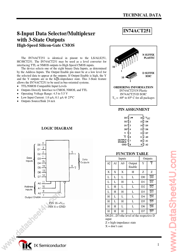
feature allows the IN74ACT251 to be used in bus-oriented systems.
- TTL/NMOS patible Input Levels
- Outputs Directly Interface to CMOS, NMOS, and TTL
- Operating Voltage Range: 4.5 to 5.5 V
- Low Input Current: 1.0 µA; 0.1 µA @ 25°C
- Outputs Source/Sink 24 m A
ORDERING INFORMATION IN74ACT251N Plastic IN74ACT251D SOIC TA = -40° to 85° C for all packages
PIN ASSIGNMENT
LOGIC DIAGRAM
FUNCTION TABLE
Inputs A2 X L L L L H H H A1 X L L H H L L H A0 X L H L H L H L Output Enable H L L L L L L L Outputs Y Z D0 D1 D2 D3 D4 D5 D6 Y Z D0 D1 D2 D3 D4 D5 D6 w w w
.d h s a t a ee
. u t4
PIN 16 =VCC PIN 8 = GND m o c
H H H L D7 D7 D0,D1...D7=the level of the respective D input Z = high-impedance state X = don’t care
..
MAXIMUM RATINGS-
Symbol VCC VIN VOUT IIN IOUT ICC PD Tstg TL
- Parameter DC Supply Voltage (Referenced to GND) DC Input Voltage (Referenced to GND) DC Output Voltage (Referenced to GND) DC Input Current, per Pin DC Output Sink/Source Current, per Pin DC Supply Current, VCC and GND Pins Power Dissipation in Still Air, Plastic DIP+ SOIC Package+ Storage Temperature Lead Temperature, 1 mm from Case for 10 Seconds (Plastic DIP or SOIC Package)
Value -0.5 to +7.0 -0.5 to VCC +0.5 -0.5 to VCC +0.5 ±20 ±50 ±50 750 500 -65 to +150 260
Unit V V V m A m A m A m W °C °C
Maximum Ratings are those values beyond which damage to the device may occur. Functional operation should be restricted to the Remended Operating Conditions. +Derating
- Plastic DIP:
- 10 m W/°C from 65° to 125°C SOIC Package: :
- 7 m W/°C from 65° to 125°C
REMENDED OPERATING CONDITIONS
Symbol VCC VIN, VOUT TJ TA IOH IOL tr, tf
- Parameter DC Supply Voltage (Referenced to GND) DC Input Voltage, Output Voltage (Referenced to GND) Junction Temperature (PDIP) Operating Temperature, All Package Types Output Current
- High Output Current
- Low Input Rise and Fall Time (except Schmitt Inputs)
- Min 4.5 0 -40
Max 5.5 VCC 140 +85 -24 24
Unit V V °C °C m A m A ns/V
VCC =4.5...