IN74ACT253
IN74ACT253 is Dual 4-1 Data Selector/Multiplexer manufactured by IK Semiconductor.
TECHNICAL DATA
Dual 4-Input Data Selector/Multiplexer with 3-State Otputs
High-Speed Silicon-Gate CMOS
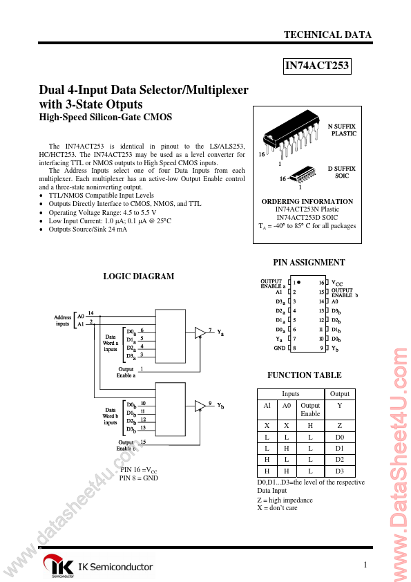
The IN74ACT253 is identical in pinout to the LS/ALS253, HC/HCT253. The IN74ACT253 may be used as a level converter for interfacing TTL or NMOS outputs to High Speed CMOS inputs. The Address Inputs select one of four Data Inputs from each multiplexer. Each multiplexer has an active-low Output Enable control and a three-state noninverting output.
- TTL/NMOS patible Input Levels
- Outputs Directly Interface to CMOS, NMOS, and TTL
- Operating Voltage Range: 4.5 to 5.5 V
- Low Input Current: 1.0 µA; 0.1 µA @ 25°C
- Outputs Source/Sink 24 m A
ORDERING INFORMATION IN74ACT253N Plastic IN74ACT253D SOIC TA = -40° to 85° C for all packages
PIN ASSIGNMENT LOGIC DIAGRAM
FUNCTION TABLE
Inputs A1 X L A0 X L H L H Output Enable H L L L L Output Y Z D0 D1 D2 D3 w w w
.d e e h s a t a
. u t4 m o c
PIN 16 =VCC PIN 8 = GND
D0,D1...D3=the level of the respective Data Input Z = high impedance X = don’t care
..
MAXIMUM RATINGS-
Symbol VCC VIN VOUT IIN IOUT ICC PD Tstg TL
- Parameter DC Supply Voltage (Referenced to GND) DC Input Voltage (Referenced to GND) DC Output Voltage (Referenced to GND) DC Input Current, per Pin DC Output Sink/Source Current, per Pin DC Supply Current, VCC and GND Pins Power Dissipation in Still Air, Plastic DIP+ SOIC Package+ Storage Temperature Lead Temperature, 1 mm from Case for 10 Seconds (Plastic DIP or SOIC Package)
Value -0.5 to +7.0 -0.5 to VCC +0.5 -0.5 to VCC +0.5 ±20 ±50 ±50 750 500 -65 to +150 260
Unit V V V m A m A m A m W °C °C
Maximum Ratings are those values beyond which damage to the device may occur. Functional operation should be restricted to the Remended Operating Conditions. +Derating
- Plastic DIP:
- 10 m W/°C from 65° to 125°C SOIC Package: :
- 7 m W/°C from 65° to 125°C
REMENDED OPERATING CONDITIONS
Symbol VCC VIN, VOUT TJ TA IOH IOL tr, tf
- Parameter DC Supply Voltage (Referenced to GND)...