IN74LV02
IN74LV02 is Quad 2-Input NOR Gate manufactured by IK Semiconductor.
TECHNICAL DATA
Quad 2-Input NOR Gate
The IN74LV02 is a low-voltage Si-gate CMOS device that is pin and function patible with 74HC/HCT02A, 74ALS02 Features
:
- Wide Operating Voltage: 1.0~5.5 V
- Input voltage levels are patible with standard CMOS levels
- Accepts TTL input levels between VCC =2.7 V and VCC =3.6 V
- Output voltage levels are patible with input levels C-MOS, N-MOS and TTL microcircuits.
- Maximum input current : 1.0 mA
ORDERING INFORMATION IN74LV02N DIP IN74LV02D SOIC
- Consumption current : 8 mA.
TA = -40° to 125° C for all packages
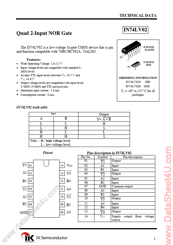
IN74LV02 truth table
Input
A L L H H
B L H L H
Output Y= A + B H L L L
Note
- H
- high voltage level;
Pinout
Y1...