IN74LV240
IN74LV240 is Octal Buffer/line Driver manufactured by IK Semiconductor.
TECHNICAL DATA
OCTAL BUFFER/LINE DRIVE; 3-STATE
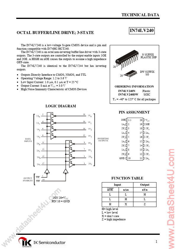
The IN74LV240 is a low-voltage Si-gate CMOS device and is pin and function patible with IN74HC/HCT240. The IN74LV240 is an octal non-inverting buffer/line driver with 3-state outputs. The 3-state outputs are controlled by the output enable inputs 1OE and 2OE. A HIGH on n OE causes the outputs to assume a high impedance OFF-state. The IN74LV240 is identical to the IN74LV244 but has inverting outputs.
- -
- -
- Outputs Directly Interface to CMOS, NMOS, and TTL Operating Voltage Range: 1.2 to 3.6 V Low Input Current: 1.0 µA, 0.1 µА at Т = 25 °С Output Current: 8 m A at VCC = 3.0 V High Noise Immunity Characteristic of CMOS Devices
N SUFFIX PLASTIC DIP
1 20 1
DW SUFFIX SO
ORDERING INFORMATION IN74LV240N IN74LV240DW Plastic SOIC
TA = -40° to 125° C for all packages
LOGIC DIAGRAM
1A0 1A1 1A2 1A3 2A0 2A1 2 4 6 8 11 13 18 16 14 12 9 7 5 3 1Y0 1Y1 1Y2 1Y3 2Y0 2Y1 2Y0 2Y1
PIN ASSIGNMENT
1OE 1A0 2Y3 1A1
INVERTING OUTPUTS
1 2 3 4 5 6 7 8 9 10
20 19 18 17 16 15 14 13 12 11
VCC 2OE 1Y0 2A3 1Y1 2A2 1Y2 2A1 1Y3 2A0
DATA INPUTS
2Y2 1A2 2Y1 1A3 2Y0 GND
2A0 15 2A1 17
OUTPUT ENABLES
1OE 2OE
1 19
FUNCTION TABLE
Input Output n An L H X n Yn H L Z n OE L L H w w a d . w e h s a t
4 t e u. m o c
PIN 20=VCC PIN 10 = GND
H= high level L = low level X = don’t care Z = high impedance
..
MAXIMUM RATINGS-
Symbol VCC IIK
- IO
- ICC IGND PD
1 2
Parameter DC supply voltage DC Input diode current DC Output diode current DC Output source or sink current DC VCC current DC GND current Power dissipation per package:
- Plastic DIP SO Storage Temperature Lead Temperature, 1.5 mm (Plastic DIP Package), 0.3 mm (SO Package) from Case for 4...