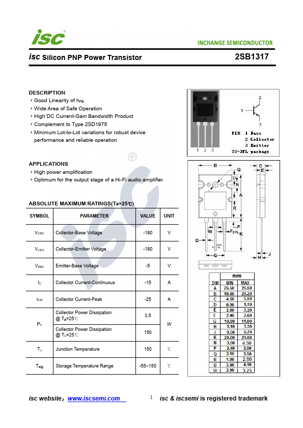
Good Linearity of hFE
Wide Area of Safe Operation
High DC Current-Gain Bandwidth Product
Complement to Type 2SD1975
Minimum Lot-to-Lot variations for robust device
performance and reliable operation
APPLICATIONS
High power amplification
Optimum for the output stag
The following content is an automatically extracted verbatim text
from the original manufacturer datasheet and is provided for reference purposes only.
View original datasheet text
isc Silicon PNP Power Transistor
2SB1317
DESCRIPTION ·Good Linearity of hFE ·Wide Area of Safe Operation ·High DC Current-Gain Bandwidth Product ·Complement to Type 2SD1975 ·Minimum Lot-to-Lot variations for robust device
performance and reliable operation
APPLICATIONS ·High power amplification ·Optimum for the output stage of a Hi-Fi audio amplifier.
ABSOLUTE MAXIMUM RATINGS(Ta=25℃)
SYMBOL
PARAMETER
VALUE UNIT
VCBO
Collector-Base Voltage
-180
V
VCEO
Collector-Emitter Voltage
-180
V
VEBO
Emitter-Base Voltage
-5
V
IC
Collector Current-Continuous
-15
A
ICM
Collector Current-Peak
Collector Power Dissipation
@ Ta=25℃ PC
Collector Power Dissipation @ TC=25℃
TJ
Junction Temperature
-25
A
3.