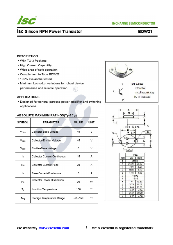
With TO-3 Package
High Current Capability
Wide area of safe operation
Complement to Type BDW22
100% avalanche tested
Minimum Lot-to-Lot variations for robust device
performance and reliable operation
APPLICATIONS
Designed for general-purpose power amplifier and sw
The following content is an automatically extracted verbatim text
from the original manufacturer datasheet and is provided for reference purposes only.
View original datasheet text
isc Silicon NPN Power Transistor
INCHANGE Semiconductor
BDW21
DESCRIPTION ·With TO-3 Package ·High Current Capability ·Wide area of safe operation ·Complement to Type BDW22 ·100% avalanche tested ·Minimum Lot-to-Lot variations for robust device
performance and reliable operation
APPLICATIONS ·Designed for general-purpose power amplifier and switching
applications.
ABSOLUTE MAXIMUM RATINGS(Ta=25℃)
SYMBOL
PARAMETER
VALUE
UNIT
VCBO
Collector-Base Voltage
VCEO VEBO
IC
Collector-Emitter Voltage Emitter-Base Voltage Collector Current-Continuous
ICM
Collector Current-Peak
IB
Base Current-Continuous
PC
Collector Power Dissipation
TJ
Junction Temperature
Tstg
Storage Temperature Range
45
V
45
V
6
V
15
A
20
A
5
A
90
W
150
℃
-55~150
℃
isc website:www.iscsemi.