IPB16CN10NG
Overview
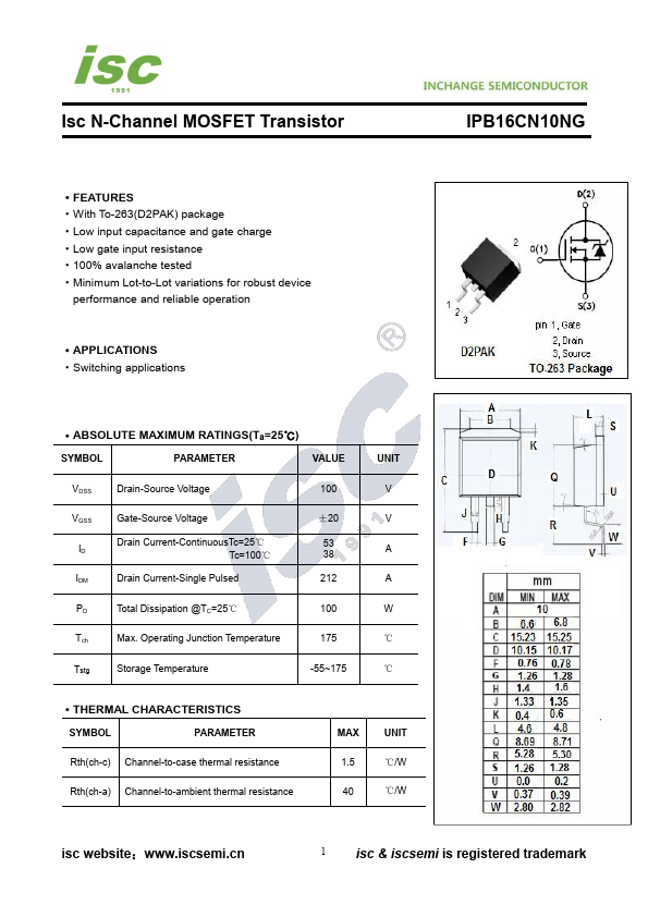
- With To-263(D2PAK) package
- Low input capacitance and gate charge
- Low gate input resistance
- 100% avalanche tested
- Minimum Lot-to-Lot variations for robust device performance and reliable operation
| Part | IPB16CN10NG |
|---|---|
| Description | N-Channel MOSFET |
| Category | MOSFET |
| Manufacturer | Inchange Semiconductor |
| Size | 254.11 KB |