SPA16N50C3 Overview
Key Specifications
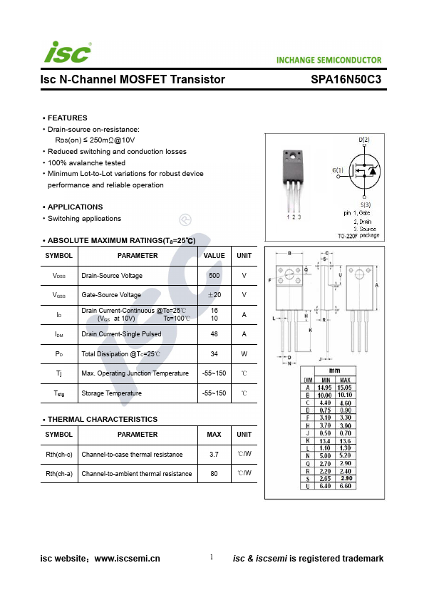
Mount Type: Through Hole
Pins: 3
Max Operating Temp: 150 °C
Min Operating Temp: -55 °C
Key Features
- Drain-source on-resistance: RDS(on) ≤ 250mΩ@10V
- Reduced switching and conduction losses
- 100% avalanche tested
- Minimum Lot-to-Lot variations for robust device performance and reliable operation