STP25N10F7
STP25N10F7 is N-Channel MOSFET manufactured by Inchange Semiconductor.
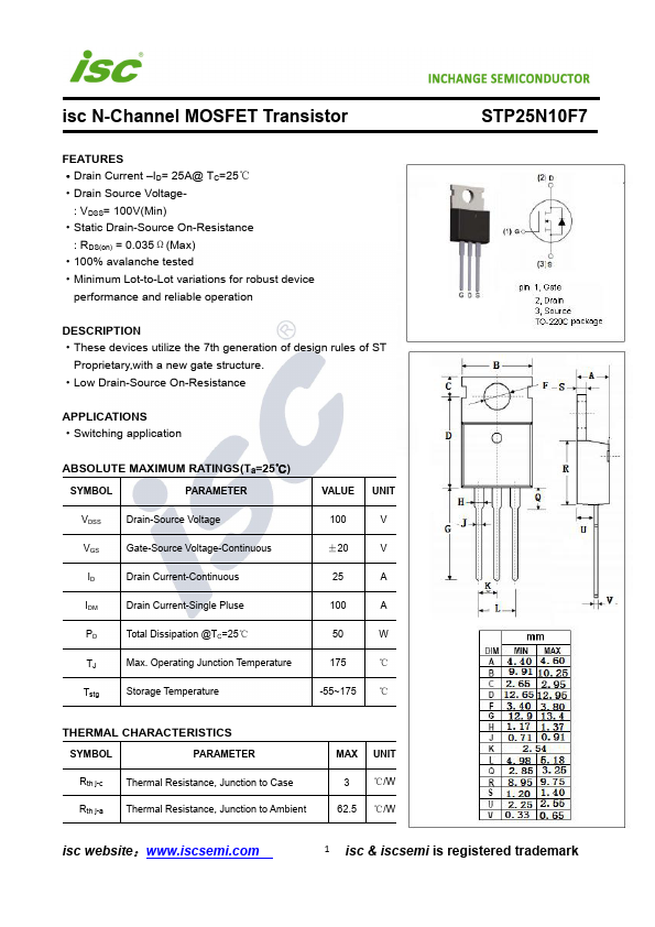
isc N-Channel MOSFET Transistor
Features
- Drain Current
- ID= 25A@ TC=25℃
- Drain Source Voltage-
: VDSS= 100V(Min)
- Static Drain-Source On-Resistance
: RDS(on) = 0.035Ω(Max)
- 100% avalanche tested
- Minimum Lot-to-Lot variations for robust device performance and reliable operation
DESCRIPTION
- These devices utilize the 7th generation of design rules of ST
Proprietary,with a new gate structure.
- Low Drain-Source On-Resistance
APPLICATIONS
- Switching...