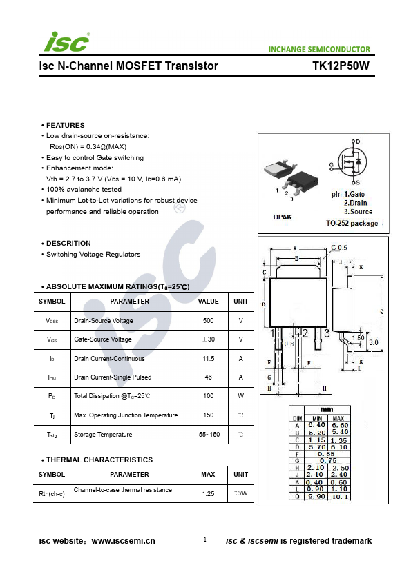
Datasheet4U Logo Datasheet4U.com

TK12P50W - N-Channel MOSFET

Key Features

  • Low drain-source on-resistance: RDS(ON) = 0.34Ω(MAX).
  • Easy to control Gate switching.
  • Enhancement mode: Vth = 2.7 to 3.7 V (VDS = 10 V, ID=0.6 mA).
  • 100% avalanche tested.
  • Minimum Lot-to-Lot variations for robust device performance and reliable operation.

📥 Download Datasheet

Full PDF Text Transcription (Reference)

The following content is an automatically extracted verbatim text from the original manufacturer datasheet and is provided for reference purposes only.

View original datasheet text
isc N-Channel MOSFET Transistor TK12P50W ·FEATURES ·Low drain-source on-resistance: RDS(ON) = 0.34Ω(MAX) ·Easy to control Gate switching ·Enhancement mode: Vth = 2.7 to 3.7 V (VDS = 10 V, ID=0.6 mA) ·100% avalanche tested ·Minimum Lot-to-Lot variations for robust device performance and reliable operation ·DESCRITION ·Switching Voltage Regulators ·ABSOLUTE MAXIMUM RATINGS(Ta=25℃) SYMBOL PARAMETER VALUE UNIT VDSS Drain-Source Voltage 500 V VGS Gate-Source Voltage ±30 V ID Drain Current-Continuous 11.5 A IDM Drain Current-Single Pulsed 46 A PD Total Dissipation @TC=25℃ 100 W Tj Max. Operating Junction Temperature 150 ℃ Tstg Storage Temperature -55~150 ℃ ·THERMAL CHARACTERISTICS SYMBOL PARAMETER Rth(ch-c) Channel-to-case thermal resistance MAX 1.