TK12P50W
TK12P50W is N-Channel MOSFET manufactured by Toshiba.
MOSFETs Silicon N-Channel MOS (DTMOS)
1. Applications
- Switching Voltage Regulators
2. Features
(1) Low drain-source on-resistance: RDS(ON) = 0.265 Ω (typ.) by used to Super Junction Structure : DTMOS
(2) Easy to control Gate switching (3) Enhancement mode: Vth = 2.7 to 3.7 V (VDS = 10 V, ID = 0.6 mA)
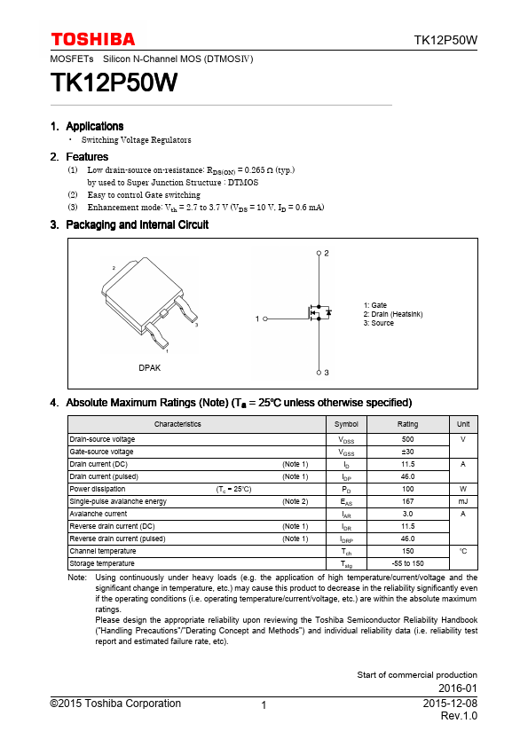
3. Packaging and Internal Circuit
1: Gate 2: Drain (Heatsink) 3: Source
DPAK
4....